Special Process PCB
- Home
- Special Process PCB
PCB Manufacturing
and PCB Assembly
KKPCB conducts research on special processing technologies such as ordinary double-sided boards, thick copper circuit boards, high-frequency circuit boards, HDI circuit boards, rigid-flexible circuit boards, FPC flexible boards, buried blind hole circuit boards, and IC carrier boards. Provides PCB design, PCB layout, PCB prototyping and PCB assembly services.
Heavy copper PCB
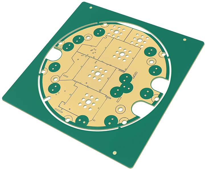
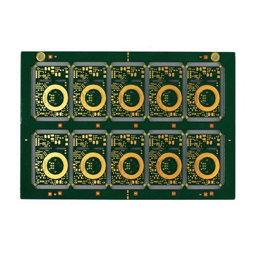
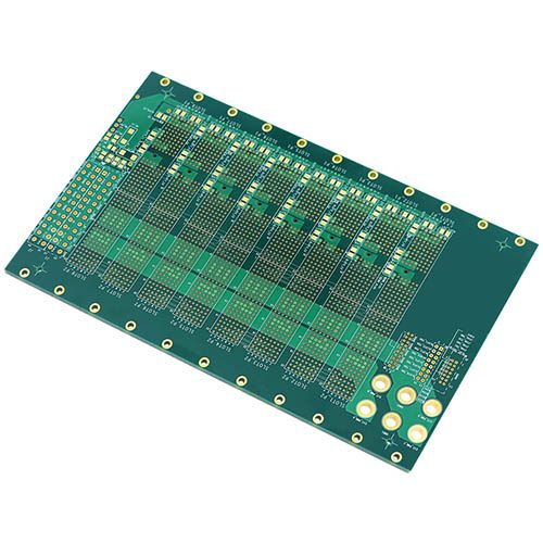
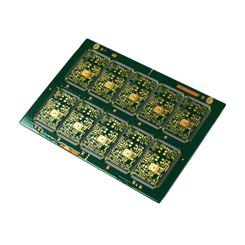
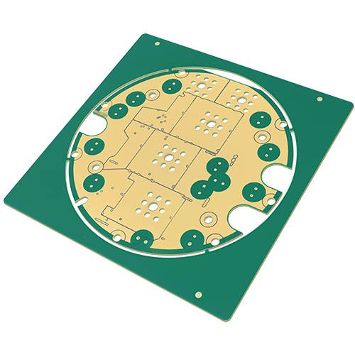
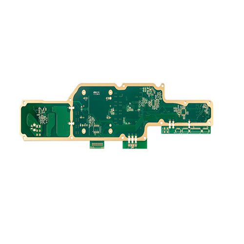
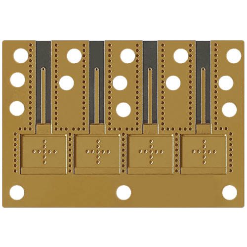
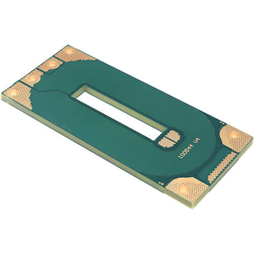
Heavy copper usually means the copper foil thickness of PCB higher than 3 ounce (4 mil or 100 micron). It mostly used for high power (electric current) electronics like power supply or some power circuit in automotive industry. It can be design in inner layer or outer layer. In PCB production, it is more difficult than traditional circuits with copper foil less than 2 ounce.

Heavy Copper PCB Capabilities:
- Heavy copper pcb copper weight up to 68OZ
- Number of layers up to 32 layers
- Heavy copper pcb Board thickness up to 10 mm
- Inner layer Cu thicknesses of 105 µm, 210 µm, or 1050 µm depending on current load
- Variable outer layer Cu thicknesses of 50 µm – 1050 µm
- Complex high-current structures possible
- Up to 4 x 1050 µm Cu per PCB possible
- Many years of series production experience with 400 µm Cu on inner layers
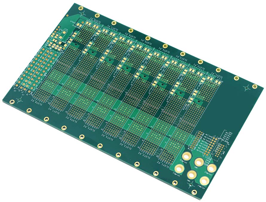
Etching of pattern is one of the major issue need to overcome for heavy copper PCB. When the copper thickness become thicker, the etching process time will be longer. When the etching solution remove the copper vertically, it will also cause side etching simutaneously. Finally, the pattern will have a big “foot” which have much smaller width on the top than on the bottom. It always reduce the copper volume used to transfer current. To meet the design criteria, PCB fabricator needs to make trace width compensation first so that the line width can pass the specification. It means a wider trace space is also important. When the copper thickness higher than 5 ounce, the problem become more difficult. The thicker the copper foil, the wider the design trace/space width is a common perception.
The second process to be concerned is the lamination. To fill the space being etched off, it needs a lot of resin to fill in. Usually the resin need to come from the prepreg. So the PCB fabricator is always use multiple high resin content prepreg in heavy copper construction. However, it will cause many problems.
- The total thickness will become high. If the prepreg used is too less, it may cause the void inside. But too many prepreg may cause the total thickness or dielectric thickness between layer out of specification.
- During lamination, the multiple high resin content prepreg will have high resin flow and cause the inner layer shift. The layer-to-layer mis-registration will become a problem for fabricator to overcome.
- the resin rich area may have resin crack issue for its no reinforcement. The higher CTE also cause some reliability issue in higher temperature.
The third issue need to be concerned is the drilling. When the design has many thick copper, the drilling parameter need to adjust to more similar to drill a thick copper plate. The drill bit wear and debris removal need to be process carefully.
The forth problem is on the solder mask process. It’s difficult to apply enough solder mask to cover thick copper pattern and base material with severe height difference. Usually, manufacturer need to fill more solder mask to fill in the space between the trace. It’s common to apply multiple printing. The first printing fill most of the pattern gap and second printing cover enough thick of solder mask on the trace pattern. But it still have some risk of voiding. The thick solder mask is also more difficult to exposure and develop. If the exposure energy is too weak, then some undercut problem may happen.
One issue that power supply designer looked is the high potential test (Hi-Pot Test). To get enough insulation to resist high voltage testing, the material, multilayer stack-up, inner layer cleaness, etching and design are all important. Sometimes the drilling, routing and plating also play an important role to get good electrical insulation.
When the copper thickness go even higher like 10 ounce or higher, the manufacturing process needs to make some change. Manufacturer can apply some resin on the trace gap first to prevent too much resin filling or the risk of voiding. This is also the key to manufacture multiple thick of copper pattern on one layer.
Applications which require running a high power we offer heavy and extreme copper tracing, plated through holes (PTH), surface pads and ground planes. By electroplating heavier copper to your pcb you are insuring high reliability and efficient power distribution. In fact, we have found that heavy copper tracing can even act as its own heat exchanger dissipating as much as 20% of overall temperature. Extreme copper thickness can be plated as high as 30oz.
HEAVY COPPER PCB APPLICATIONS:
- High Power Distribution
- Planar Transformers
- Heat Dissipation
- Power Converters
- Amplification Systems
- Solar Panel Manufactures
- Power Controllers
- Welding Equipment
Heavy copper PCB Products:
- High Current PCB
- Thick Copper PCB (105-240μm)
- Ultra Thick Copper PCB (300-500μm)
- Ultra Max Thick Copper PCB (2185μm)
- Combination PCB
- Bus Bar Embedded PCB
- Copper Inlay PCB
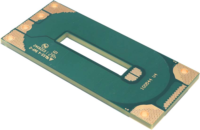
Bus bar metal PCB board including:
- Embedding bus bar into inner layer
- Extracting copper and bending copper
- Embedding into external layer
- The shape of bus bar is flexible
- Heavy copper metal PCB support up to 500 Amps
- Available copper thickness is up to 2000um.
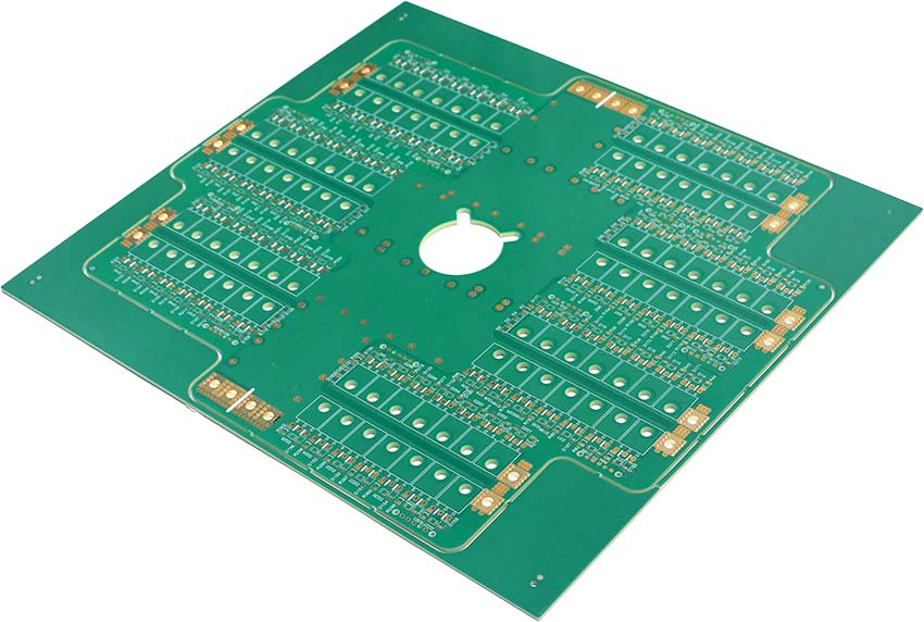
Bus Bar Embedded PCB Applications:
- Replacement of Bus Bar
- High voltage high current terminal board
- High Voltage Breaker
- Small Mobility
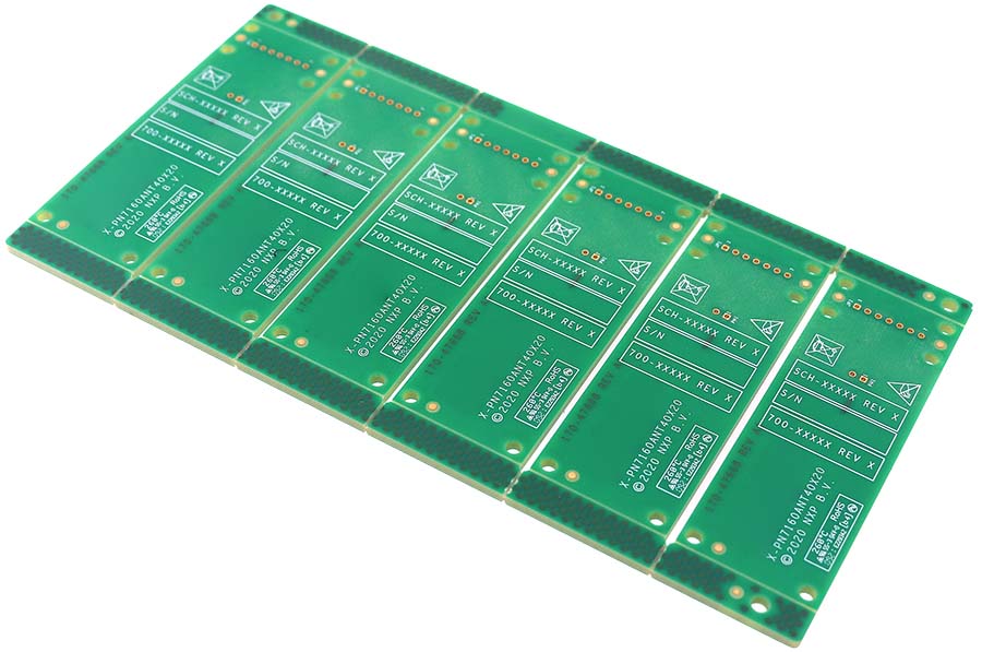
Bus Bar Embedded PCB Manufacturer
Higher currents require tailored copper profiles in PCBs. Because installation space is always limited, the Z-axis must be utilised. With inner layer copper thicknesses of up to 400 µm, applications with continuous currents of more than 200 A are possible.
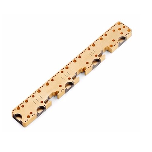
Instead of using etching process to make conductive traces, 2185um(86oz) or heavier Bus-Bar is made of rolled copper foils by metal fabrication, and it can be embedded in PCB.
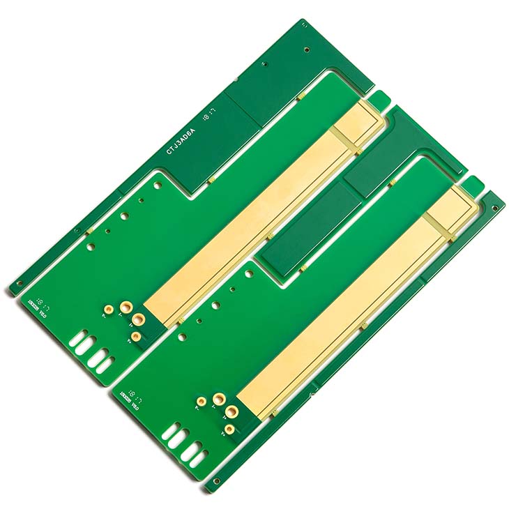
In case of conventional High Current PCB, it is necessary to use thick base copper, so material cost is increased, and price of PCB becomes expensive. Total PCB cost can be reduced because Bus Bar is used only necessary area where you would like to use. Also it is possible to mount parts on the bus bar by combining Bus Bar and PCB.
Heavy copper PCBs, manufactured in genuine etching technology, are the first choice in case of high currents and characterised by structures with copper thicknesses from 105 to 400 µm.
This PCB classic is the first choice when high currents are unavoidable: the heavy copper PCB, manufactured in genuine etching technology. Heavy copper PCBs are characterised by structures with copper thicknesses from 105 to 400 µm. These PCBs are used for large (high) current outputs and for optimisation of the thermal management. The heavy copper allows large PCB-cross-sections for high current loads and encourages heat dissipation. The most common designs are multilayer or double-sided. With this PCB technology it is also possible to combine fine layout structures on the outer layers and heavy copper layers in the inner layers.
We are happy to support your heavy copper PCB project at every step along the way.

