Special process for PCB processing of circuit boards
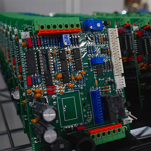
Special process flow for PCB processing of circuit boards As a practitioner in the PCB industry, for PCB copying, PCB design-related processes must be mastered. Through the analysis of our company’s professional PCB copying experts, our professional PCB copying experts have sorted out the following special process flow for PCB processing of circuit boards for you, hoping to help PCB industry practitioners.
Additive process addition
Refers to the process of directly growing a local conductor line with a chemical copper layer on the surface of a non-conductor substrate with the help of an anti-corrosion agent (see the 47th issue of the Circuit Board Information Journal, page 62). The additive method used for PCB copying can be divided into different methods such as full additive method, semi-additive method and partial additive method.
Backplane, backplane support plate
It is designed to be used to plug in other thicker boards (such as 0.093″, 0.125″), and the method is to first insert a multi-pin connector in a tight through hole, but without soldering, and then pass the connector through the guide pins of the board one by one for wiring. Common PCB copying, just insert the connector. Because the through holes of this special board cannot be welded, but are directly clamped with the hole wall and the guide pin, the quality and aperture requirements are particularly strict. The number of orders is small, and general circuit board factories are unwilling to accept such orders, and it is difficult to accept them. It has become a high-end specialized industry in the United States.
Establishment process
This is a new field of thin multilayer board practice. The earliest inspiration came from IBM’s SLC process, which was implemented by its Yasu factory in Japan in 1989. This method is based on the traditional double-sided board. The surface of the outer layer is fully coated with a liquid photosensitive precursor such as Probmer 52. After semi-hardening and photosensitization, a shallow “photoconductive via” (Photo-Via) that communicates with the next bottom layer is made. Then, chemical copper and electroplated copper are fully added to the conductor layer. After line imaging and etching, a new type of wire and buried or blind hole interconnected with the bottom layer can be obtained. Repeated stacking can obtain a multilayer board with the required number of layers. This method not only saves the expensive mechanical drilling costs, but also reduces the aperture to less than 10mil. In the past five or six years, various multilayer board technologies that break through traditional reforms have been promoted by American, Japanese, and European companies, making these Build Up Processes famous, with more than ten products on the market, of various types.
In addition to the above-mentioned “photosensitive holes”, there are also different basic chemical methods such as biting holes, laser ablation, and plasma etching. After removing the copper in the holes, organic boards are used to make via holes. In addition, there is a new type of “Resin Coated Copper Foil coated with semi-hardened resin”, which can be used to make thinner, denser, smaller, and thinner multilayer boards using the Sequential Lamination method. In the future, diversified personal electronic products will become the world of this truly thin and short multilayer board.
Metal ceramics are made by mixing ceramic powder and metal powder, and then adding adhesive as a coating. They are printed on the surface (or inner layer) of the circuit board in the form of thick film or thin film printing to form a “resistor”, which can be directly mounted during assembly to replace external resistors.
Co-firing Co-firing
It is a process for the manufacture of hybrid PCB circuit boards (Hybrid), which uses a variety of precious metal film thick film pastes (Thick Film Paste) printed on a small board surface. The various organic carriers in the thick film paste are burned off, leaving the precious metal conductor wires as interconnected wires.
Crossover, the two vertical and horizontal lines on the board surface are crossed in three dimensions, and the gaps at the intersection are filled with insulating media. Generally, adding carbon film jumpers to the green paint surface of a single-sided board, or wiring underneath using the build-up method are all considered “crossover”.
Scattered wire board Scattered PCB board, double-sided board
That is to say, a multi-layer circuit board is a board with round enameled wires and through holes. The performance of a double-layer board in high-frequency transmission lines is better than that of a general PCB etched rectangular line.
DYCOstrate Plasma Hole Layering
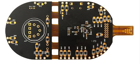
It is a Build Up Process developed by Dyconex in Zurich, Switzerland. First, the copper foil of each hole on the board is removed, placed in a closed vacuum environment, and filled with CF4, N2, and O2 to ionize it under high voltage to form a highly active plasma. This patented method can etch a perforated substrate with tiny through holes (less than 10 mil), which is commercially called DYCOstrate.
Electrodeposition Photoresist Electroresist, Electrophoretic Photoresist
It is a new type of “photosensitive resist” process, which was originally used in the “electrical paint” of complex metal objects, and has only recently been introduced into the application of “photoresist”. The colloidal charged resin charged colloidal particles are evenly plated on the copper surface of the PCB circuit board by electroplating as an anti-etching resist. At present, mass production has begun on the process of direct etching of copper in the inner layer. This type of ED photoresist can be placed in the anode or cathode method according to different operation methods, and is called “anode type electroresist” and “cathode type electroresist” respectively. In addition, according to the principle of photosensitivity, there are two types: “photopolymerization” (negative working) and “photodecomposition” (positive working). At present, negative working ED photoresist has been commercialized, but it can only be used as a planar resist. In the through hole, image transfer cannot be used for the outer layer due to the difficulty of photosensitivity. As for the “positive ED” that can be used as an outer layer photoresist (because it is a photosensitive decomposition film, the photosensitive body is insufficient but not affected), the Japanese industry is still stepping up its efforts to commercialize it and use it in mass production to make it easier to achieve fine line production. This term is also called “electrophoretic photoresist”.
Flush Conductor Embedded Circuit, Flat Conductor
It is a special PCB copy board with a completely flat appearance and all conductor circuits pressed into the board. The method of making a single-sided board is to first etch the copper foil on the semi-cured substrate by image transfer to obtain the circuit, and then press the board circuit into the semi-cured board by high temperature and high pressure, and complete the hardening of the board resin at the same time. The circuit board is pressed into the surface to become a completely flat circuit board. Usually, on the surface of the circuit that has been pressed into the circuit board, a thin copper layer needs to be micro-etched and then a 0.3mil nickel layer is plated, as well as a 20 micro-inch thick gold layer or a 10 micro-inch thick gold layer. When sliding contact is made, the contact resistance is low and it is easier to slide. However, this method is not suitable for PTH, in order to prevent the through hole from being crushed during pressing, and it is not easy to achieve a completely flat board surface, and it cannot be used at high temperature to prevent the resin from expanding and pushing out the circuit. This technology is also called Etch and Push method, the full name is Flush-Bonded Board, which can be used for special purposes such as Rotary Switch and Wiping Contacts.
In addition to precious metal chemicals, the Frit glass powder in the Poly Thick Film (PTF) slurry also needs glass powder to solidify and adhere under high-temperature incineration, so that the slurry on the blank ceramic substrate can form a solid precious metal circuit system.
Full Additive Process
It is a “full additive method”, that is, on the surface of a completely insulating thin sheet, a selective circuit is grown by electroless metal deposition (mostly chemical copper). Another less correct statement is the “full electroless” method.
Hybrid Integrated Circuit Hybrid Circuit
It is a circuit carrier formed by coating precious metal conductive ink on a small ceramic thin substrate, and then burning the organic matter in the ink at high temperature to leave the conductor line on the board surface, and welding the surface glue part. It is a circuit carrier of thick film technology between printed circuit boards and semiconductor integrated circuit devices. In the early days, it was mostly used for military or high-frequency purposes. In recent years, due to the high price and the reduction of military use, as well as the difficulty of automated production, coupled with the increasing miniaturization of circuit boards, this type of hybrid growth has been much worse than in the early years.
Interposer
Any two layers of conductors carried by insulating objects are called interposers by filling them with some conductive fillers. For example, in the bare holes of multilayer boards, if silver paste or copper paste is used to replace the orthodox copper hole wall, or a vertical unidirectional conductive adhesive layer, etc., these are interposers.
Laser direct imaging, LDI laser direct imaging
The boards with laminated dry films are no longer transferred by film exposure, but are directly exposed to the dry film by fast scanning photosensitivity instead of computer-directed laser beams. Since the parallel light emitted is concentrated in a single beam of energy, the side walls of the dry film after development can be made more vertical. However, this method can only operate on each board separately, so the mass production speed is not as fast as using film and traditional exposure. LDI can only produce 30 medium-sized boards per hour, so it can only appear occasionally on prototype proofing or high-priced boards. Due to its inherent high cost, it is difficult to promote in the industry.
Laser Processing Laser Processing
There are many precise processes in the electronics industry, such as cutting, drilling, welding, soldering, etc., which can also be performed with the energy of laser light, which is the so-called laser processing. The so-called LASER is the abbreviation of “light amplified stimulated radiation”. The mainland industry translates it as “laser”, which is more appropriate than transliteration. Laser was invented by American physicist TH Maiman in 1959. It uses a single beam of light to irradiate ruby to generate laser light. After years of research, a new processing method has been created. In addition to the electronics industry, it can also be used for medical and military purposes.
Micro Wire Board Micro-sealed (wrapped) board
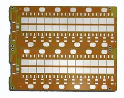
A special circuit board that attaches circular enameled wire (glue wire) to the board surface and uses PTH to complete the interconnection between layers is commonly known as Multiwire Board in the industry. When the wiring density is very large (160~250in/in2) and the wire diameter is very small (below 25mil), it is also called a micro-sealed circuit board.
Moulded Circuit Molded 3D Circuit Board
The process of making 3D circuit boards by using 3D molds, injection molding or deformation is called Moulded Circuit or Moulded Interconnection Circuit. The left picture is a schematic diagram of MIC after two injections.
Multi-circuit board (or discrete circuit board)
Refers to a multi-layer interconnected circuit board obtained by winding extremely fine enameled wire directly on the copper foil-free surface, and then fixing it with glue, drilling and electroplating holes. This was developed by PCK in the United States and is currently produced by Hitachi in Japan. This MWB saves design time and is suitable for small quantities and complex circuit models (there is a special article in the 60th issue of Circuit Board Information Magazine).
Precious metal paste Precious metal paste
It is a conductive paste for thick film circuit printing. When it is printed on a ceramic substrate by screen printing, fixed precious metal lines appear after the organic carrier is burned off at high temperature. The conductive metal powder added to the paste must be a precious metal to avoid the formation of oxides at high temperatures. The product users are gold, platinum, rhodium, palladium or other precious metals.
Pad-only board
In the early days of through-hole insertion, some high-reliability multi-layer boards only left through holes and solder rings outside the board to ensure solderability and circuit safety, and hid the interconnection lines in the next inner layer. This type of double-layer board will not be printed with solder mask green paint, and the appearance is particularly exquisite, and the quality inspection is also extremely strict. At present, due to the increase in wiring density, many portable electronic products (such as mobile phones) only leave SMT pads or a few lines on the surface of the circuit board, and the interconnection dense lines are buried in the inner layer. The layers are also replaced by more difficult blind holes or “Pads On Hole” as interconnections to reduce the damage of all through holes to the ground and voltage copper. This SMT method is also a type of pad.
Polymer Thick Film (PTF) Thick Film Paste
Refers to the precious metal paste used to make circuits on ceramic substrate thick film circuit boards, or the printing paste to form printed resistor films. The process includes screen printing and subsequent high-temperature incineration. After the organic carrier is burned off, a well-attached circuit system appears, which is usually called a hybrid circuit.
Semi-additive method Semi-additive method
It refers to the process of growing the required circuit directly on the surface of the insulating substrate with chemical copper, and then continuing to thicken it by electroplating copper. It is called a “semi-additive” process. If the thickness of all circuits is thickened by chemical copper, it is called a “full-additive” process. Note that the above definition comes from the latest IPC-T-50E promulgated in July 1992, which is different from the original IPC-T-50D (November 1988). The early “D version” and the general industry saying is on a non-conductive bare substrate, or on a substrate covered with thin copper foil (such as 1/4 ounce or 1/8 ounce thin foil), prepare for negative resistance image transfer, and thicken the required circuit by chemical copper or electroplating copper.

