


Solder Paste and Stencil Considerations for Double-Sided PCBs
Designing double-sided PCBs requires careful planning to ensure efficient assembly, high yields, and reliable solder joints. Solder paste application and stencil design play a critical role in achieving these goals. This article explores key considerations for solder paste and stencil design, focusing on double-sided PCBs, component orientation, and advanced techniques for fine-pitch devices.
Key Considerations for Double-Sided PCB Assembly
1. Component Orientation and Spacing
- Consistency is Key: Rotate components consistently and space them evenly to improve solderability and assembly efficiency.
- Electrical vs. Manufacturing Priorities: While electrical performance often dictates component placement, aligning the majority of components in a uniform orientation can streamline the assembly process.
- Tombstone Defect Prevention: Proper orientation helps reduce tombstone defects, especially for passive components.
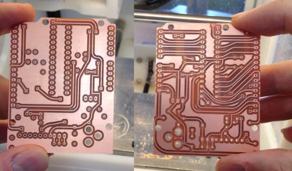
2. A/B Flip Panels for Double-Sided Assembly
- Efficiency in Manufacturing: A/B flip panels allow both sides of a double-sided PCB to be assembled simultaneously using a single stencil and pick-and-place file.
- Balanced Assembly Time: By flipping half the panel 180 degrees, the time required to populate both sides becomes equal, even if one side has more components.
- Component Weight Considerations: Heavier components on the bottom side may require adhesive to prevent detachment during reflow, but this can increase costs and rework complexity.
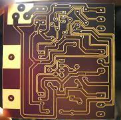
3. Stencil Design and Solder Paste Application
- Stencil Thickness: Typical stencil thickness is 4 mils, but finer-pitch devices may require thinner stencils (e.g., 3 mils) to control solder paste volume.
- Laser-Cut Stencils: Laser cutting ensures precision for fine-pitch components, with options for stepped stencils to apply varying solder paste volumes.
- Solder Paste Formulations: Particle size and composition (e.g., SAC305) affect reflow performance. Finer particles are better suited for small apertures.
Solder Mask Defined (SMD) vs. Non-Solder Mask Defined (NSMD) Pads
1. Solder Mask Defined Pads
- Use Case: Ideal for fine-pitch devices where solder mask bridges between pads are necessary.
- Design Considerations: The solder mask opening matches the pad size, and the stencil aperture is adjusted to control solder volume.
- Advantages: Prevents solder bridging and ensures consistent solder joint formation.
2. Non-Solder Mask Defined Pads
- Use Case: Suitable for larger components where solder mask alignment is less critical.
- Design Considerations: The copper pad extends beyond the solder mask, allowing for larger stencil apertures.
- Advantages: Simplifies design and improves solder joint strength.
Advanced Techniques for Fine-Pitch Components
1. Organic Pad Shapes
- D-Shaped Pads: For ultra-small components like 01005 passives, D-shaped pads with rounded corners improve solder joint reliability.
- Home Plate Pads: Tilted or rotated pads reduce solder paste volume under fine-pitch gaps, minimizing bridging.
2. Solder Mask Adjustments
- Mask Extensions: Reduce solder mask extensions (e.g., from 50 microns to 37 microns) for smaller components.
- Trace Routing: Adjust solder mask around traces to maintain pad integrity and prevent solder wicking.
3. Solder Paste Volume Control
- Stepped Stencils: Apply varying solder paste volumes across the board to accommodate different component sizes.
- Aperture Design: Use smaller apertures for fine-pitch components and larger apertures for power components.
Practical Tips for Double-Sided PCB Assembly
1. Tooling Holes and Fiducial Marks
- Ensure tooling holes and fiducial marks are present on both sides of the panel for accurate alignment during assembly.
2. Test Coupons and Indicators
- Include test coupons and directional arrows in the discard area to guide assembly and testing processes.
3. Reflow Profile Optimization
- Adjust reflow temperatures based on solder paste formulation and component sensitivity.
- Run pilot projects to identify and address solder defect trends.
Double-sided PCB assembly requires a balance between design efficiency, manufacturability, and solder joint reliability. By optimizing component orientation, leveraging A/B flip panels, and employing advanced stencil techniques, designers can achieve high yields and reduce costs. Understanding the nuances of solder paste application and stencil design is essential for delivering high-quality, reliable PCBs in both prototyping and high-volume production.
KKPCB conducts research on special processing technologies such as ordinary double-sided boards, thick copper circuit boards, high-frequency circuit boards, HDI circuit boards, rigid-flexible circuit boards, FPC flexible boards, buried blind hole circuit boards, and IC carrier boards. Provides PCB design, PCB layout, PCB prototyping and PCB assembly services.