SMT Assembly Instructions: A Beginner’s Guide
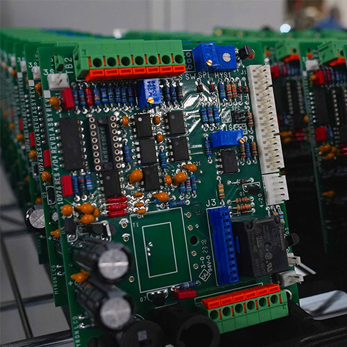
Electronic devices have transformed our lives, from smartphones to electric vehicles, all thanks to continuous innovation and advancements in technology. At the heart of these devices are printed circuit boards (PCBs) that are meticulously manufactured, assembled, and packaged to deliver the final products we rely on. This article explores the PCB Surface Mount Technology (SMT) assembly process, detailing its steps, benefits, and common challenges.
What is SMT Assembly?
Before diving into SMT assembly, it’s essential to understand what a printed circuit board (PCB) is.
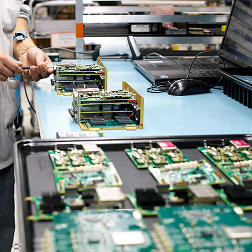
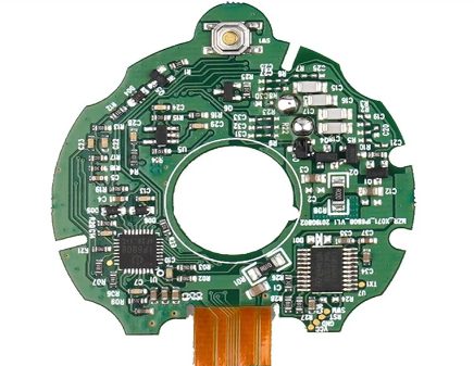
A PCB is a substrate or laminate that supports and connects electronic components to enable various device functionalities. Common substrates include FR4 (flame retardant material), but there are alternatives such as polyimide for flexible designs. PCBs are categorized by layers—single-sided, double-sided, and multi-layer—and by substrate type (rigid, flexible, or rigid-flex combinations).
Surface Mount Technology (SMT) is a method of assembling components onto the PCB surface, replacing the traditional Through-Hole Technology (THT), which involves inserting component leads through PCB holes. SMT PCB assembly is favored for its advantages in high-density designs, offering better space utilization, efficiency, and reliability.
Processes Involved in SMT Assembly
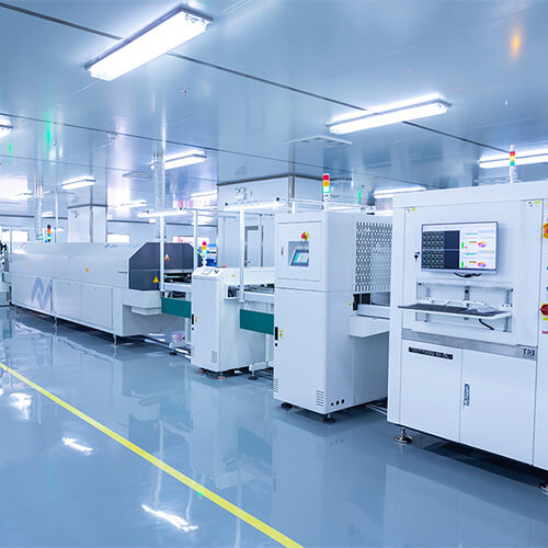
SMT assembly is a streamlined and highly automated process. Here’s a breakdown of its key steps:
1. Stencil Printing
- Objective: Apply solder paste onto the PCB surface using a stencil and scraper.
- Process: The solder paste is evenly distributed into the stencil’s holes, aligning with the PCB pads. Variables like solder paste viscosity, squeegee pressure, printing speed, and stencil separation speed must be controlled for consistency.
- Impact: Approximately 60% of defects in SMT assembly arise from stencil printing issues. Post-printing, the solder paste undergoes inspection to ensure uniformity.
2. Component Placement
- Objective: Precisely place electronic components on the soldered PCB.
- Process: Automated pick-and-place machines use vision systems to identify and position components accurately. These systems utilize cameras, lighting, and fiducials (markers) to guide placement.
- Key Considerations: Optimal speed, alignment, and noise reduction are critical for efficient placement.
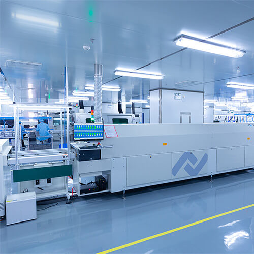
3. Reflow Soldering
- Objective: Secure components by melting the solder paste.
- Process: The PCB passes through a reflow oven with controlled temperature zones: ramp, preheat, peak reflow, and cool-down. An inert nitrogen atmosphere minimizes oxidation.
- Quality Indicators: Successful solder joint formation with minimal voids and adequate wetting of contact pads.
4. Quality Inspection
- Automated Optical Inspection (AOI): Compares PCBs to reference images for defects. Challenges include false positives or missed errors.
- X-Ray Inspection: Identifies solder voids and internal defects not visible through AOI. Essential for multilayer PCBs and high-density designs.
Common Defects in SMT Assembly
Despite its precision, SMT assembly faces certain recurring defects:
- Solder Bridging
- Cause: Excess solder paste creates shorts between adjacent components.
- Solution: Monitor solder paste volume during stencil printing.
- Tombstoning
- Cause: Uneven solder wetting causes components to tilt.
- Solution: Ensure even temperature, paste distribution, and surface tension.
- Missing Components
- Cause: Errors in pick-and-place setup or component misselection.
- Solution: Regular calibration and verification of machine setups.
- Misaligned Components
- Cause: Shifts during placement or reflow.
- Solution: Use fiducials for precise alignment and inspect placement accuracy.
- Solder Voids
- Cause: Contaminated contact pads or expired solder paste.
- Solution: Maintain proper reflow profiles and ensure clean materials.
Conclusion
SMT assembly is a cornerstone of modern electronics manufacturing, offering unparalleled efficiency and versatility for high-density PCB designs. While challenges like solder defects and component misalignment exist, advancements in automated processes and inspection technologies continue to enhance SMT reliability. As technology evolves, SMT assembly will remain at the forefront of PCB manufacturing, adapting to new requirements and further optimizing its capabilities.


