


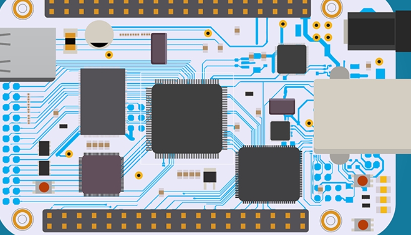
Simple Strategies for Double Sided 2-Layer PCBs
Many times we discuss complex boards with unique features and sensitive routing on this blog. But the reality is that most PCBs that are mass manufactured have lower layer counts and less complexity. 2-layer PCBs will continue to be high-volume products, and they are almost always the starting point for a new designer learning about PCB layout. In some ways, 4-layer boards make things much easier because they include internal plane layers, and it can be easy to make simple mistakes on 2-layer boards due to the lack of ground and space for routing.
Because many designers will need to build a 2-layer board at some point, we will outline some simple approaches that can help prevent common mistakes in 2-layer boards. One of the big reasons we use 2-layer boards is because they can quickly scale to high volume, but this can also demand EMC compliance as well as other forms of compliance. Some of the guidelines we will discuss here are intended to aid EMI suppression as this is one of the big concerns in taking a product to market.
2-Layer Board Approaches
2-layer boards can be single-sided or double-sided. The guidelines discussed here assume double-sided placement, where components are on both sides of the board. However, this could also apply to single-sided placement with routing in both layers, something which is common in many 2-layer designs.
No matter where the components are placed in the PCB, you may find some of these common approaches to building 2-layer PCBs.
Place Ground Everywhere With Copper Pours
Ground is key to a 2-layer board with digital and mixed-signal circuits working correctly. Without a clear definition of ground, it will not be possible to predict return paths in the PCB or sufficiently address EMI suppression needs.
The simplest way to implement this is to place a large copper pour everywhere on the top and bottom layers of the PCB. This will ensure that every signal has a ground return nearby, which will help ensure the design can still pass EMC testing.
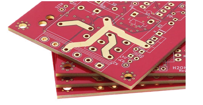
Avoid Excessively Large Power Rails
2-layer boards always lack space for large bunches of traces and large rails. This means that large power rails should usually be avoided in these designs. Large rails for power can take up excessive amounts of space, and instead wide traces can be used to provide power to components. Wide traces can still handle considerable current; for example, a good rule-of-thumb is a 100-10 rule, meaning a 100 mil wide trace is appropriate for 10 A of current without excessive heating.
Every rule has exceptions, and there are some simple boards where the above points about rails do not apply. For example, in power electronics that do not have digital or configuration lines, most of the components will be electromechanical or inductive. These boards also tend to carry a lot of current. Therefore, these 2-layer PCBs might need large rails, and they will usually have enough room that the rails can easily fit into the PCB.
Try to Avoid Overlapping Signals
2-layer boards always lack space, so there is sometimes a tendency to unintentionally bring signals too close together on different layers. Depending on the signals involved, this can create a risk of crosstalk or noise coupling in general. When routing the components in the board, try to plan routes ahead of time so that parallel signals are avoided on each side of the board.
Instead, use right-angle routing or orthogonal routing, where traces are routed in perpendicular directions. For example, the top layer can be used for vertical routing, and the bottom layer can be used for horizontal routing.
Smart Placement and Layout
The best way to ensure a board will be functional and noise-free, while also scaling to volume production, is with smart placement decisions. The above practices do not magically solve noise problems, and the locations of important components still need to be selected so that noise does not couple between different circuits. With the right placement practices, you can separate components from each other such that they do not create noise or interference.
This is all about following mixed-signal design practices. Here are some resources where you can learn more:
- Overview of mixed-signal circuit design
- Mixed-signal PCB design guidelines
- Mixed-signal PCB routing tips
KKPCB conducts research on special processing technologies such as ordinary double-sided boards, thick copper circuit boards, high-frequency circuit boards, HDI circuit boards, rigid-flexible circuit boards, FPC flexible boards, buried blind hole circuit boards, and IC carrier boards. Provides PCB design, PCB layout, PCB prototyping and PCB assembly services.