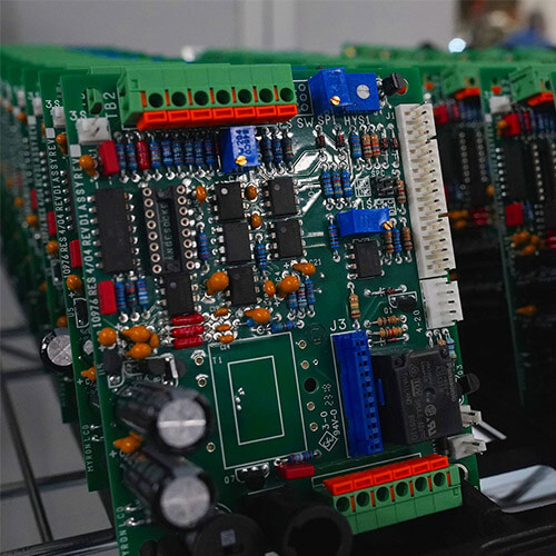
Fabrication Guidelines for RT-duroid® 5870 and 5880 High-Frequency Circuit Materials
RT-duroid® 5870 and 5880 materials are widely used for high-frequency and microwave circuit designs due to their excellent dielectric properties and low loss. However, their PTFE-based composition and unique mechanical characteristics require specific handling and fabrication processes to maintain performance and reliability.
1. Material Overview
Key Properties:
- RT-duroid 5870:
- Dielectric constant (ϵr\epsilon_rϵr): 2.33 ± 0.02.
- Dissipation factor (tanδ\tan \deltatanδ): 0.0012.
- RT-duroid 5880:
- Dielectric constant (ϵr\epsilon_rϵr): 2.20 ± 0.02.
- Dissipation factor (tanδ\tan \deltatanδ): 0.0009.
Both materials feature low moisture absorption, excellent thermal stability, and compatibility with high-frequency applications.
2. Storage and Handling
- Store in a clean, dry environment at room temperature to prevent contamination and moisture absorption.
- Use gloves to handle laminates, avoiding fingerprints or surface oils.
- Avoid bending the material, as the PTFE base is prone to deformation.
3. Cutting and Machining
3.1 Cutting:
- Use carbide or diamond-coated tools for precision.
- Shearing is not recommended due to potential delamination.
3.2 Drilling:
- Use sharp, carbide-tipped drill bits with high speed and low feed rates.
- Maintain low pressure to avoid burr formation and delamination.
- For plated through-holes (PTH), clean drilled holes with plasma or chemical etching to remove debris.
4. Copper Cladding and Etching
4.1 Copper Cladding:
- RT-duroid materials typically come with rolled or electro-deposited copper foil.
- Avoid excessive mechanical stress during processing, as the adhesion between PTFE and copper is sensitive.
4.2 Etching:
- Use standard etching solutions (e.g., ferric chloride or ammonium persulfate).
- Maintain precise temperature and agitation during etching to ensure uniform copper removal.
- Post-etch, clean thoroughly to remove chemical residues.
5. Lamination and Bonding
- Bonding Films: For multilayer applications, use Rogers 3001 or compatible bonding films designed for PTFE materials.
- Pressing: Maintain uniform pressure and temperature (typically 250°C to 350°C) during lamination.
- Release Films: Use non-stick release films to prevent damage during pressing.
6. Metallization and Plating
- PTFE surfaces require surface roughening for proper metallization.
- Use plasma treatment or sodium etching to enhance adhesion.
- Follow with electroless copper plating before electroplating to ensure uniform coverage and strong bonding.
7. Soldering and Thermal Management
7.1 Soldering:
- Use lead-free or low-temperature solders to minimize thermal stress.
- Keep soldering temperatures below 260°C to prevent PTFE degradation.
- Limit dwell time during reflow soldering to reduce warping and adhesion loss.
7.2 Thermal Relief:
- After soldering, implement stress-relief cycles (e.g., 200°C for 1 hour) to mitigate residual thermal stress.
8. Inspection and Testing
- Visual Inspection: Check for surface defects, delamination, and debris.
- Peel Strength Testing: Evaluate copper adhesion to ensure durability.
- Electrical Testing: Verify impedance and dielectric performance using a network analyzer.
9. Common Challenges and Solutions
| Challenge | Solution |
|---|---|
| Poor copper adhesion | Use plasma treatment or sodium etching before metallization. |
| Burr formation during drilling | Use sharp carbide tools and clean drilled holes with plasma etching. |
| Warping after soldering | Implement thermal stress relief after soldering. |
| Impedance mismatches | Use precise etching and tightly control dielectric constant tolerances. |
10. Safety and Environmental Considerations
- Ensure proper ventilation during plasma treatment and soldering.
- Dispose of etching chemicals and debris following environmental regulations.


