


Routing Traces in PCBs: Best Practices
PCB routing involves laying out traces to minimize interference, ensure signal integrity, and meet design requirements such as impedance control and thermal management. Traces carry electrical signals between components such as integrated circuits, resistors, and capacitors. PCB traces are usually made of copper. They are created by applying a layer of photosensitive material onto a copper-clad board, exposing it to ultraviolet light through a mask to define the circuit pattern, and then etching away the unexposed copper to leave behind the traces. They are essential for your circuit to function properly as they provide the paths for the flow of electric current.
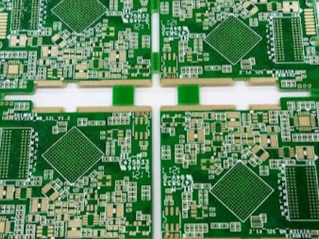
Good routing practices include optimizing trace widths, avoiding sharp corners and right angles, and maintaining appropriate separation between traces. The table below lists the best practices for routing traces on a PCB.
| Best Practices for Routing Traces in PCBs | |
| Planning | Plan the placement of components and the general routing strategy to maximize performance and minimize interference. |
| Critical Signals | Route critical signals first to ensure they have the shortest and most direct paths on the PCB. |
| Design Guidelines | Follow the design guidelines specified by the PCB manufacturer to ensure the PCB manufacturability and reliability. |
| Signal Crosstalk | Reduce signal crosstalk and interference by keeping high-speed signal traces apart. Separate analog and digital signals as much as possible. |
| Trace Lengths | Shorten trace lengths to reduce signal propagation delays and minimize signal degradation. |
| Trace Widths | Choose trace widths based on the signals’ current carrying capacity and impedance requirements. Ensure trace widths are consistent so that impedance remains controlled and signals are not reflected. |
| Ground and Power Planes | Use ground planes and power planes to provide low-impedance return paths and reduce electromagnetic interference (EMI). |
| Sensitive Signals/Noisy Components | Keep sensitive analog signals away from noisy digital components to minimize interference and improve signal integrity. |
| Signal Integrity | Ensure that the routed signals meet the required timing and voltage levels by performing signal integrity analysis. |
| Testing | Test the PCB design using simulations or prototypes before manufacturing to identify any issues. |
Routing Traces in PCBs to Ensure Signal Integrity
Ensuring signal integrity through proper routing is essential to PCB design. Here are some important routing considerations to improve signal integrity:
- Signal Requirements: Begin by understanding the electrical characteristics of the signals you’re routing, including frequency, rise/fall times, and signal levels. This will help you make informed decisions about trace geometry, impedance, and routing topology.
- Layer Stackup Design: Design the PCB layer stackup with consideration for signal integrity. High-speed signals may require controlled impedance traces, often requiring specific layer arrangements and materials.
- Trace Length Matching: For parallel data buses or differential pairs, ensure that trace lengths are matched within specified tolerances to prevent skew and maintain signal timing integrity. Use length-matching tools in PCB layout software to achieve this.
- Impedance Control: Maintain consistent trace impedance along the signal path, which involves controlling trace width, thickness, and the dielectric constant of the PCB material. Tools such as field solvers or impedance calculators can aid in designing traces with the desired impedance.
- Crosstalk: Keep traces carrying high-speed signals adequately spaced apart to minimize electromagnetic coupling (crosstalk). Differential pairs should be routed close together with consistent spacing and parallelism to maximize common-mode noise rejection.
- Signal Integrity Analysis: Use signal integrity analysis tools to simulate the behavior of signals on the PCB. These tools can predict signal integrity issues such as reflections, crosstalk, and impedance mismatches, allowing you to optimize the design before fabrication.
- Signal Return Paths: Ensure high-speed signals have a clear and low-impedance return path to complete their circuit loop. This often involves providing a dedicated ground plane or ground traces adjacent to signal traces.
- Signal Termination: Use termination techniques such as series resistors or parallel termination to minimize signal reflections and ringing. The termination method depends on the signal type, transmission line characteristics, and system requirements.
By following these guidelines, designers can route traces to ensure signal integrity, minimize errors and maximize system reliability.