High-Speed PCB Design Guide 7: Reducing RF Effects in PCB Interconnection Design
PCB interconnections can be categorized into three main types: chip-to-PCB, interconnections within the PCB, and PCB-to-external devices. High-frequency PCB designs require addressing RF effects at these interconnection points to ensure optimal performance. This guide covers techniques for minimizing RF interference, crosstalk, and return loss across these interconnection types.
The Impact of High-Frequency Signals on PCB Design
As data rates climb, signal frequencies often exceed 1GHz, introducing RF and low-end microwave challenges. These electromagnetic (EM) fields induce unwanted effects like crosstalk, which can degrade signal integrity, and return loss caused by impedance mismatches.
Negative Impacts of Return Loss:
- Increased System Noise: Reflected signals add noise, complicating signal interpretation.
- Signal Degradation: Reflected signals alter signal shapes, leading to errors.
Achieving a return loss of -25dB or better is critical for maintaining signal integrity in high-frequency digital systems.
Strategies to Reduce RF Effects
1. Chip-to-PCB Interconnection
High-speed chips, like Pentium IV, push PCB design limits. Challenges include handling high I/O density and minimizing signal degradation. Innovations like local wireless transmitters inside chips aim to bypass traditional interconnect issues. However, PCB designs often lag behind IC advancements, making interconnection a critical area for improvement.

2. PCB Internal Interconnection
High-frequency PCB design requires meticulous planning to manage RF effects:
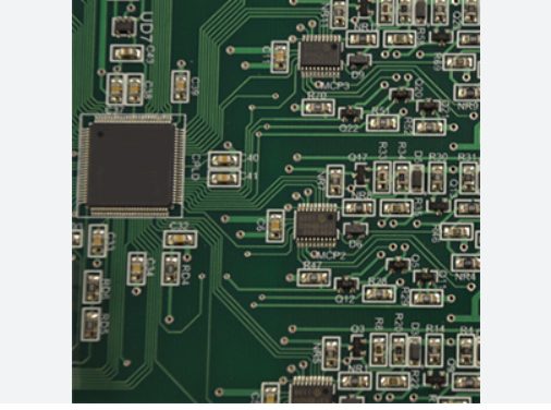
- Optimize Trace Geometry:
- Use 45° trace corners to reduce return loss.
- Adopt high-performance insulating materials to control electromagnetic fields effectively.
- Avoid Lead-Induced Inductance:
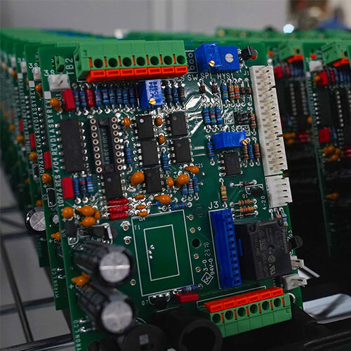
- Replace through-hole components with surface-mounted devices (SMDs).
- Minimize via processing to reduce unwanted inductance.
- Ground Layer Management:
- Incorporate dedicated ground layers connected by vias to suppress 3D EM field effects.
- Improve Plating Techniques:
- Use nickel or immersion gold plating for better high-frequency current handling compared to HASL.
- Solder Mask Considerations:
- Avoid full board coverage in microstrip designs to prevent electromagnetic field disturbances.
- Precision Etching:
- Specify line width errors to within ±0.0007 inches for controlled trace geometry.
3. PCB-to-External Device Interconnection
When connecting PCBs to external systems, maintaining impedance consistency is critical:
- Coaxial Cable Integration:
- Transition between microstrip and coaxial cables must be managed to minimize edge effects and impedance mismatches.
- Solutions from companies like Trompeter Electronics help address these transitions effectively.
- Impedance Management:
- Design for consistent impedance across PCB traces, connectors, and external cables.
- Account for frequency-dependent impedance variations during design.
The future of high-speed PCB design depends on addressing RF challenges through improved interconnection techniques, material innovations, and precision engineering. As bandwidth demands grow, mastering RF effects will remain a cornerstone of PCB development.


