Quick Reference Processing Guidelines RO3000 and RO3200 Laminates
1. Material Overview
RO3000® and RO3200® series laminates are ceramic-filled PTFE-based materials designed for RF and microwave circuit applications. These laminates offer excellent dielectric stability, low loss, and mechanical robustness, making them ideal for a wide range of high-frequency designs.
2. Key Material Properties
| Property | RO3000® Series | RO3200® Series |
|---|---|---|
| Dielectric Constant (Dk) | 3.00–10.2 | 6.15–10.2 |
| Loss Tangent (Df) | 0.0010–0.0022 | 0.0018–0.0025 |
| Coefficient of Thermal Expansion (CTE): X, Y | ~17 ppm/°C | ~22 ppm/°C |
| Thermal Conductivity | 0.50 W/m·K | 0.45 W/m·K |
3. Storage Recommendations
- Store materials flat in a cool, dry environment (20–25°C, 30–50% RH).
- Avoid exposure to direct sunlight or UV light.
- Handle with gloves to prevent contamination.
4. Drilling Guidelines
- Drill Bit Type: Use carbide or diamond-coated drill bits for optimal hole quality.
- Drilling Parameters:
- Spindle speed: 30,000–100,000 RPM.
- Feed rate: 1.5–3 mils/rev depending on material thickness.
- Stack Height: Single or small stacks recommended to reduce resin smearing.
- Deburring: Perform light deburring to maintain integrity.
5. Lamination Process
- Use prepreg or bonding films that match the thermal expansion properties of the laminates.
- Press Cycle Parameters:
- Temperature: 200–230°C (392–446°F).
- Pressure: 200–300 psi.
- Time: Minimum of 30 minutes under full pressure.
- Cool under pressure to prevent warping or delamination.
6. Etching and Patterning
- Use conventional PCB etching techniques; maintain consistency in copper thickness.
- For fine-line features, inspect patterns with automated optical inspection (AOI) equipment.
7. Plating Recommendations
- Perform thorough surface preparation, including mechanical or plasma cleaning.
- Apply electroless copper plating to ensure uniform conductivity.
- Avoid high-temperature plating processes to maintain dimensional stability.
8. Soldering and Assembly
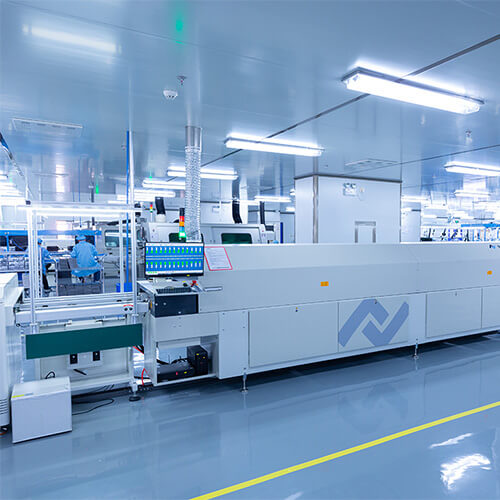
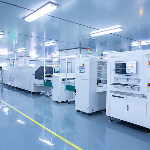
- Soldering Techniques: Use vapor phase or reflow soldering at controlled temperatures.
- Component Placement: Ensure precision placement using automated systems.
- Avoid excessive mechanical stress during assembly to maintain material integrity.
9. Testing and Inspection
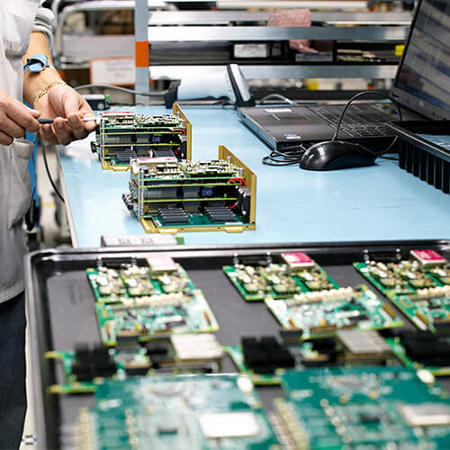
- Test for dielectric constant (Dk) and loss tangent (Df) to ensure design performance.
- Verify copper adhesion, via quality, and circuit dimensional accuracy.
- Conduct RF testing to validate electrical performance.
10. Safety and Handling Precautions
- Wear PPE during processing to protect from dust and fumes.
- Ensure proper ventilation in fabrication and assembly areas.
- Dispose of scrap material in compliance with local regulations.


