Shenzhen KKPCB Technology Co., Ltd. (KKPCB) is a professional PCB and PCBA manufacturer dedicated to providing one-stop electronic manufacturing solutions. Specializing in high-difficulty, small to medium batch PCB and PCBA production, we focus on delivering high-precision, high-reliability products with fast turnaround times to meet customers’ complex design and technical requirements.
KKPCB is definitely your trusted PCB Manufacturing and PCB Assembly partner! In addition to friendly service and on-time delivery, we also focus on producing high-quality products that meet or exceed customers’ expectations.
Lorem ipsum dolor sit amet, consectetur adipiscing elit. Ut elit tellus, luctus nec ullamcorper mattis, pulvinar dapibus leo.
Manufacturing Standards
Our technicians have many years of experience, and have been working strictly in accordance with high requirements and standards.
Quality Reports & Certifications
We can provide you with complete quality reports and common certifications as proof of the quality of our products.
Quality Control Process
We believe that only a complete quality control process is an effective means to ensure quality.
Raw Material Download
The specifications of the raw materials used in our production are available for download.
Manufacturing standards
Our experienced technicians will always ensure that all products are of exceptional quality,reliability and consistency.
PCB Standards
PCB Production standards follow IPC Class 2,IPC Class 3, ,Automotive Standard, Customer Standard
Item
Advanced PCB
Standard PCB
Engineering
one file/1 days+ Senior engineer
mid-level engineer (1 files/hours)
Material
Shengyi,Rogers,Arlon,Isola, Omega,Nelco,3M etc.Meet IPC4101 class B/L
KB(kingboard)/GDM(goldenmax) Meet IPC4101 class B/L
Forbid to repair tracks(IPC 3,Automotive,Customer Standard)
–
Cleanliness
Cleanliness requirements beyond those of IPC
Cleanliness requirements beyond those of IPC
PCB Assembly Processing Capability
PCB Assembly standards follow IPC-A-610E Standard
PCB Assembly Parameters
Bulk Order Supported Capabilities
Sample Order Supported Capabilities
PCB size
L50xW50mm~L510xW460mm
Unlimited
PCB thickness
T=0.4~4.0mm
Unlimited
Min SMD size
01005(inch)
01005(inch)
Max SMD size
45x45mm(Connector length:150mm)
Unlimited
Min IC Pin Pitch
0.3mm
0.3mm
Min BGA Ball Pitch
0.4mm
0.4mm
Equipment placement accuracy
±0.35mm @3σ
±0.35mm @3σ
SMD production capacity
1000K points/day
200 Orders/day
DIP production capacity
500K points/day
200 Orders/day
// Perfect quality system
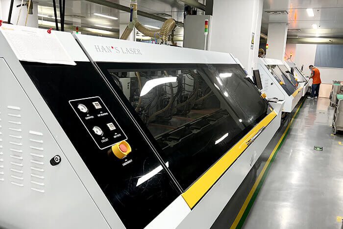
Quality Control Process
The perfect quality assurance system and various testing equipment help us monitor the entire production process to ensure the stability of the process and product quality. At the same time, we also introduce advanced instruments and technical methods to achieve continuous improvement.
PCB Quality Control Process
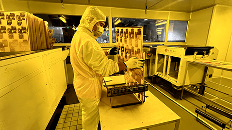
At KKPCB, quality is not just a standard—it’s our commitment. Our comprehensive PCB Quality Control Process ensures that every PCB and assembled board meets the highest industry standards for precision, durability, and reliability. By integrating advanced inspection technologies, rigorous testing protocols, and strict compliance measures, we guarantee zero-defect production and unmatched performance across all industries, including automotive, medical, aerospace, industrial, and consumer electronics.
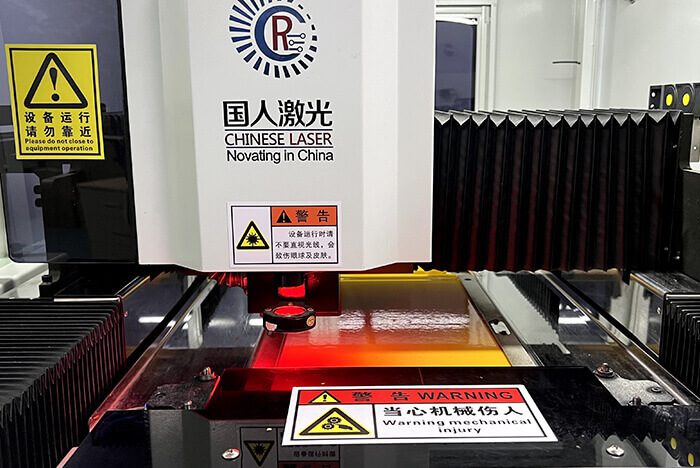
Silkscreen laser printer
Automatic dry film coating machine
FPC cover film
Lamination machine
Driling machine
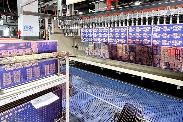
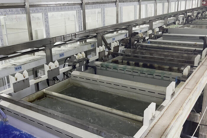
Copper plating
Electroplating
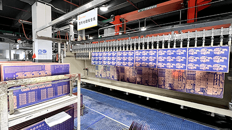
Fully automatic electroplating line
Copper plating
Our PCB Quality Control Process Includes:
1. Raw Material Inspection
Verifying PCB laminates, copper foils, and solder masks for thickness, dielectric properties, and surface integrity.
Ensuring compliance with RoHS, REACH, and UL safety and environmental regulations.
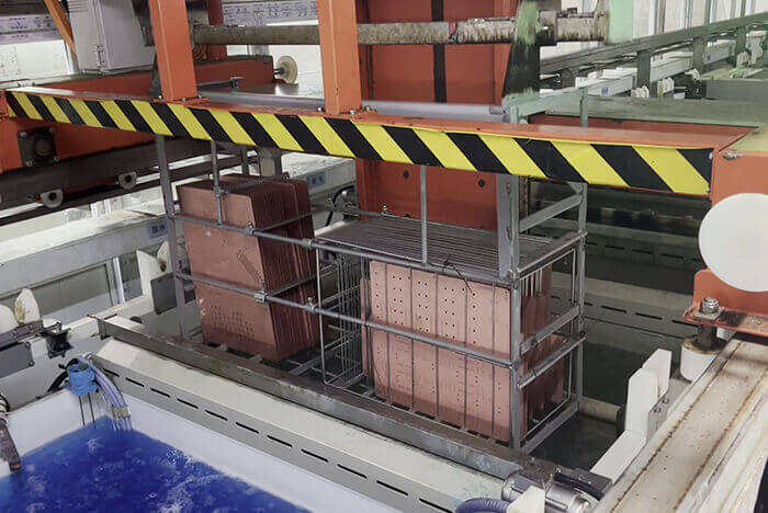
2. Inner Layer & Outer Layer Inspection
Performing Automated Optical Inspection (AOI) to detect alignment errors, etching defects, and surface contamination.
Verifying copper thickness uniformity and ensuring high-precision trace formation.
3. Drilling & Plating Quality Control
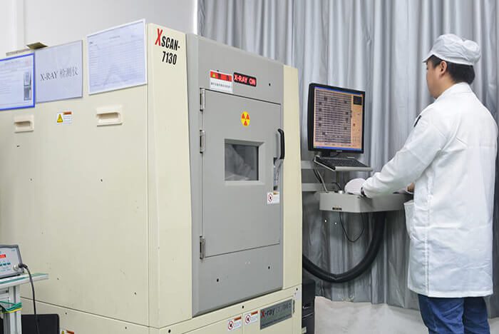
Using X-ray drilling alignment verification to ensure accurate via placement.
Conducting plating thickness measurements to meet conductivity and durability requirements.
4. Solder Mask & Silkscreen Inspection
Checking for uniform coverage, adhesion strength, and proper curing to prevent delamination.
Ensuring accurate legend printing for component identification.
5. Electrical Testing
Conducting Flying Probe & Bed-of-Nails Testing to detect shorts, open circuits, and resistance variations.
Ensuring signal integrity and impedance control for high-speed PCB applications.
6. Final Quality Assurance
Performing thermal shock, humidity resistance, and mechanical stress tests for enhanced reliability.
Ensuring every PCB meets IPC-A-600 Class 2 & Class 3 quality standards.
At KKPCB, we are committed to zero-defect PCB manufacturing, delivering high-performance, high-reliability circuit boards for applications in automotive, aerospace, medical, and industrial electronics.
At KKPCB, we implement a strict, multi-step PCB assembly quality control process to guarantee that every assembled PCB meets the highest industry standards for precision, durability, and functionality. By utilizing advanced inspection technologies, rigorous testing protocols, and certified quality management systems, we ensure zero-defect production and long-term reliability for industries such as automotive, aerospace, medical, industrial, and consumer electronics.
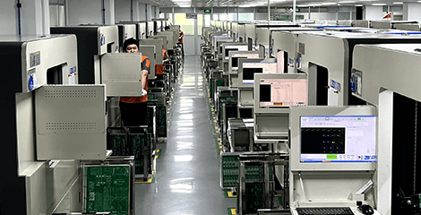
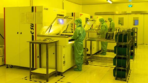
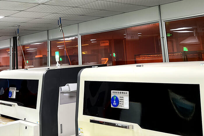
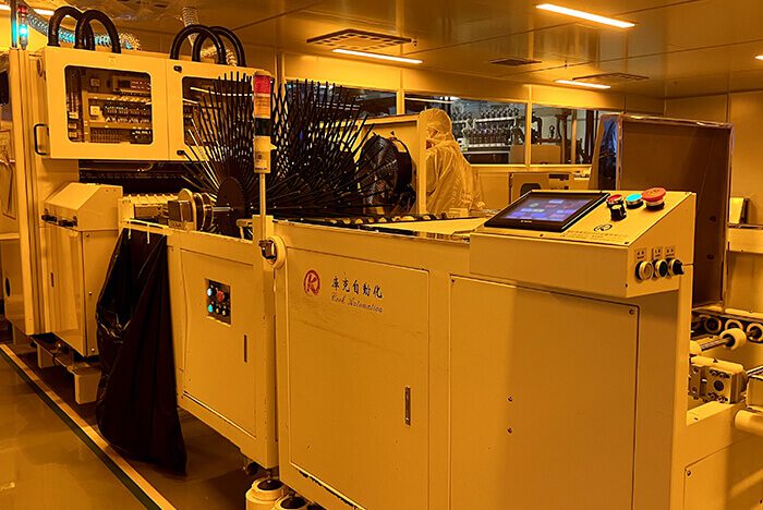
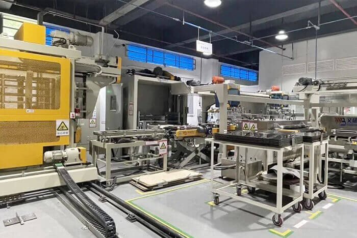
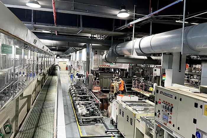
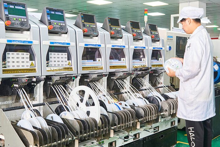
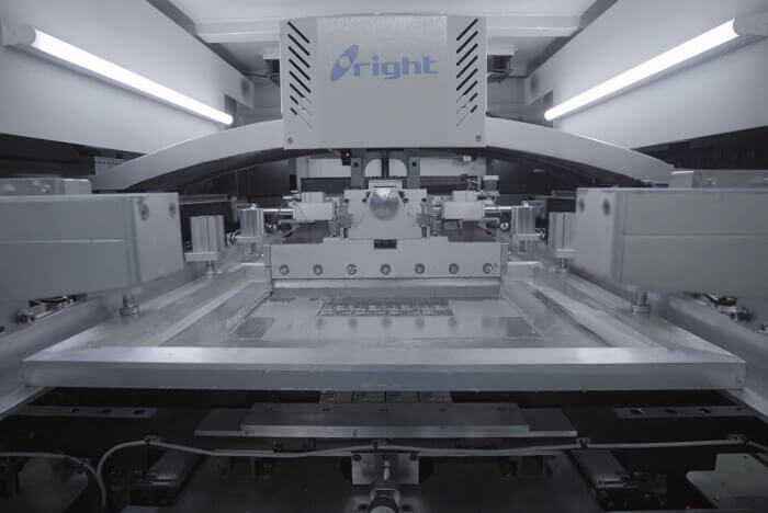
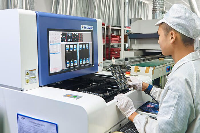
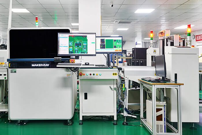
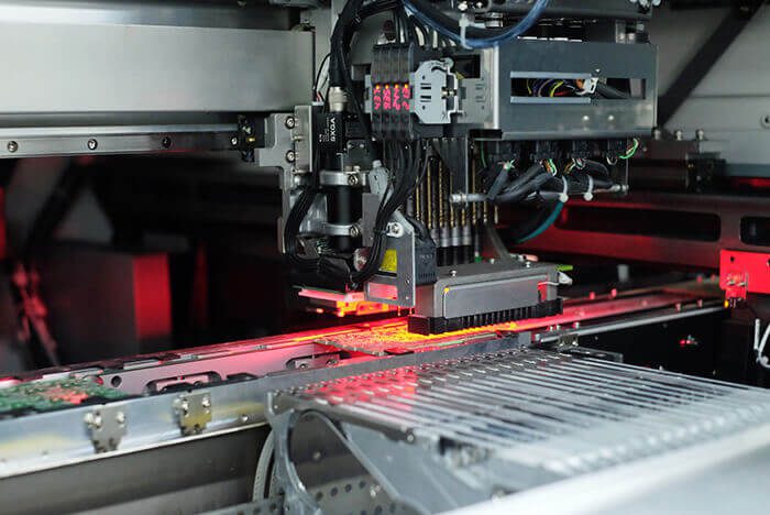
KKPCB has dozens of SMT production lines. Advanced production equipment, strict quality control and intelligent service system to ensure the standardization and best quality of each production process.
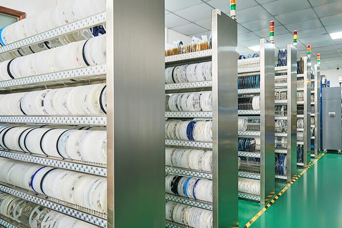
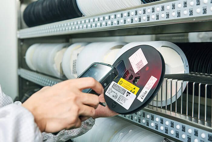
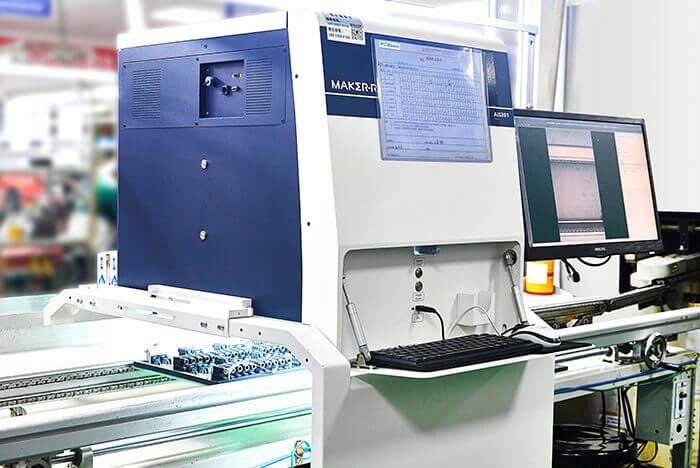
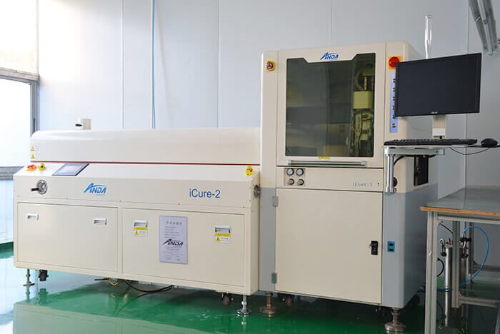
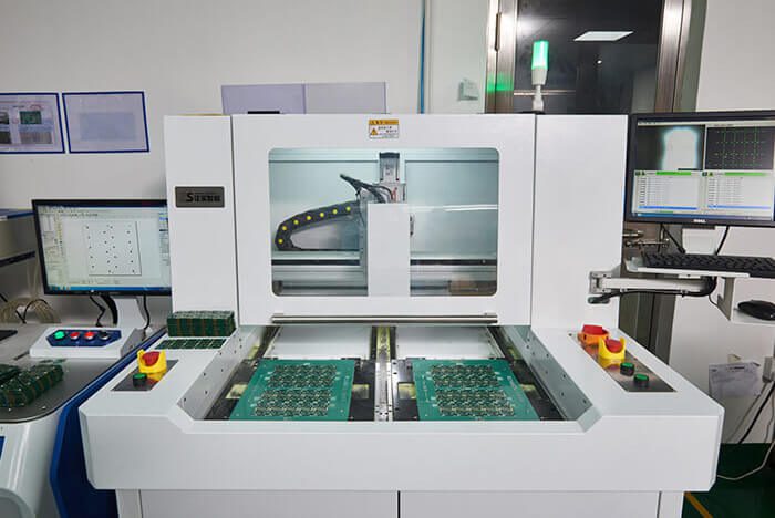
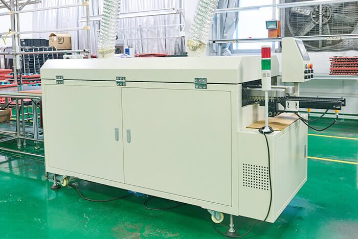
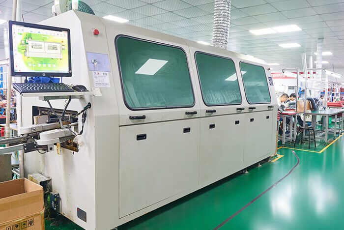
Smart management system & Advanced production and testing equipment:
High Speed Pick and Place Machine
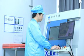
X-Ray
SPI Solder Paste
SPI
Smart Warehousing
Barcodes vs Qr Codes for InventoryManagement
AOl Machine Before the Furnace
Conformal Coating Equipment
Depaneling Machine
Microplate Washer
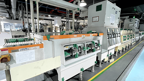
Wave Soldering
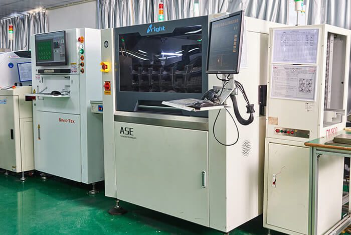
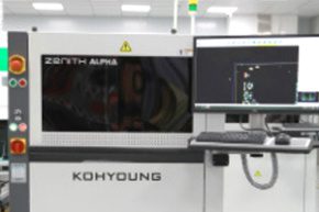
AOI
On-line AOl
SMT Placement Machine
Our PCB Assembly Quality Control Process
1. Incoming Material Inspection (IQC)
Verifying PCB bare boards, components, and solder paste for conformity with specifications (RoHS, REACH, UL, IPC standards).
Using X-ray fluorescence (XRF) and material traceability systems to ensure component authenticity and quality.
2. Solder Paste Inspection (SPI)
Ensuring precise solder paste volume, thickness, and alignment to prevent defects like bridging and insufficient soldering.
Using automated SPI systems to detect inconsistencies before placement.
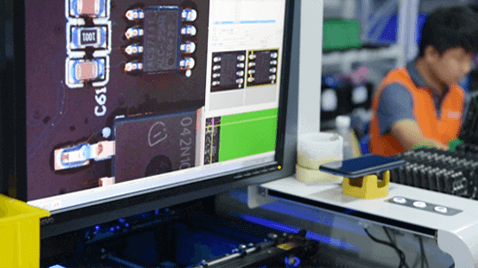
3. Automated Optical Inspection (AOI) – Pre & Post Reflow
Identifying misaligned, missing, or incorrect components during placement.
Checking for cold solder joints, insufficient solder, or bridging after reflow soldering.
4. X-ray Inspection (For BGA, QFN, and Hidden Joints)
Detecting voids, solder balling, and hidden defects in BGA, QFN, and other leadless packages.
Ensuring proper solder joint formation and connectivity.
Checking for open circuits, shorts, incorrect component values, and solder joint integrity.
Ensuring electrical connectivity and proper signal transmission.
6. Functional Testing (FCT)
Simulating real-world operating conditions to verify board functionality.
Testing power-up, microcontroller programming, signal integrity, and load performance.
7. Final Quality Assurance & Reliability Testing
Conducting burn-in testing, thermal cycling, humidity resistance, and mechanical stress testing for mission-critical applications.
Ensuring compliance with IPC-A-610 Class 2 & Class 3, ISO 9001, IATF 16949, and other industry standards.
Quality checking process and description
01-Process review
Assess and inspect the particularity of the PCBA manufacturing process in advance, guide the production, and improve the quality from the process technology.
02-IQC Incoming Quality Control
● Check whether the resistance and capacitance values are correct ● Check whether the pads on the components and the board are consistent ● Confirm whether the incoming quantity is accurate ● Check whether the components are abnormal
03-SPI Solder Paste Inspection
SPI can detect whether the solder paste is sufficient and uniform, which can effectively prevent production quality problems in advance caused by poor solder paste printing.
04-Online AOI Inspection
The AOI can detect the wrong solder, reverse solder, false solder, empty solder, incomplete solder, short circuit, offset, tombstone, etc. after reflow soldering. And it can also detect excessive solder, less solder, continuous solder and other undesirable phenomena in the appearance of PCBA solder joints.
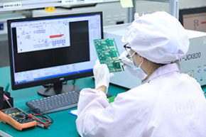
05-First sample test
Combined with Gerber, BOM and coordinate files, the resistance and capacitance in the completed PCBA are verified again by the first-sample tester to ensure the correctness of all parameter values.
06-Off-line AOI inspection
According to the IPC610D standard, inspect the soldered surface mount PCBA for errors, omissions, and false connections.
07-X-Ray welding inspection
Inspect the solder joints of invisible components to ensure the reliability of each solder ball of the BGA.
08-QC manual inspection
Refers to the standard IPC–610 inspection standard, and the finished board is visually inspected to ensure 100 % Good products shipped.
At KKPCB, our commitment to quality, precision, and reliability ensures that every assembled PCB performs flawlessly in demanding environments. With our advanced quality control systems and experienced engineering team, we deliver high-performance PCB assemblies that exceed customer expectations.
KKPCB quality management system is to ensure with efficient printed circuit boards which meet customer’s requirements. Our partners manufacture in compliance with, among others, the following standards:
IATF 16949:2016
ISO 13485:2016
IS0 14001:2015
ISO 9001:2015
ROHS
REACH
UL
CE
Thanks to the materials used and advanced technology, we always ensure highest quality of our printed circuit boards! KKPCB can provide customers with certifications in various markets, such as: EU RoHS certification, EU CE certification, US UL certification, US FCC certification, Australia SAA certification, Australia C-tick certification, Australia RCM certification, Japan PSE certification, Brazil INMETRO certification, Mexico NOM certification, Canadian IC certification, Korea lithium battery KC certification, Argentina IRAM S-mark certification, DLC certification, GS certification, CB certification, etc.