One-stop PCB Manufacturing and PCB Assembly solutions Manufacturer
- Mon - Sat: 8.00 am - 7.00 pm
- sales@kkpcb.com
One-stop PCB Manufacturing and PCB Assembly solutions Manufacturer
Over 10 years we help companies reach their financial and branding goals. Engitech is a values-driven technology agency dedicated.
411 University St, Seattle, USA
engitech@oceanthemes.net
+1 -800-456-478-23
KKPCB conducts research on special processing technologies such as ordinary double-sided boards, thick copper circuit boards, high-frequency circuit boards, HDI circuit boards, rigid-flexible circuit boards, FPC flexible boards, buried blind hole circuit boards, and IC carrier boards. Provides PCB design, PCB layout, PCB prototyping and PCB assembly services.
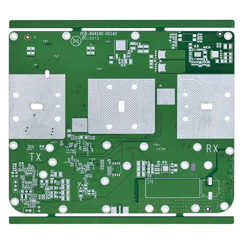
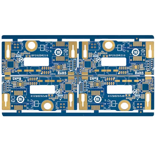
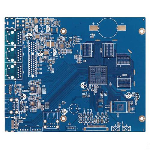
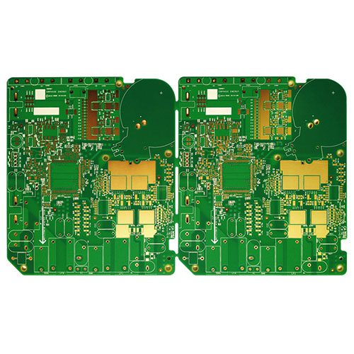
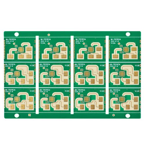
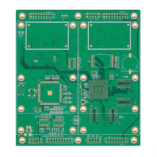
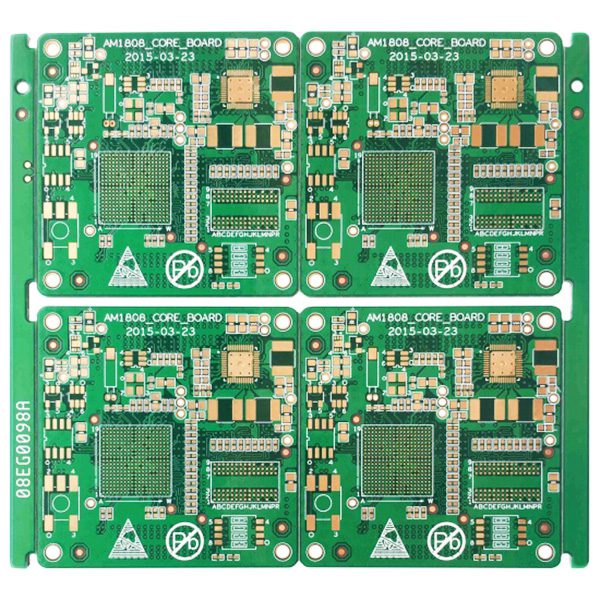
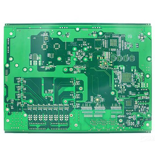
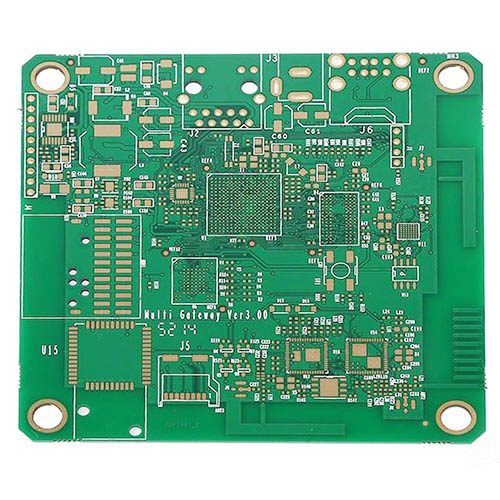
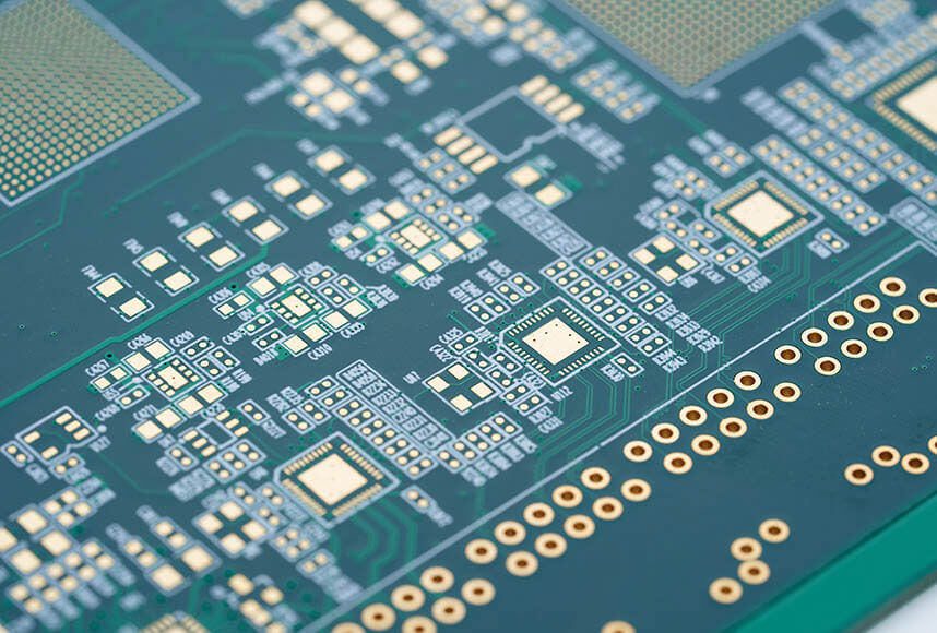
Select KKPCB as your rapid prototype manufacturer for a seamless experience. Our commitment to quality and efficiency ensures your project’s success. We offer high-end equipment, experienced engineers, and aligned production. All these factors can turn your designs into functional prototypes .
We have a proven history of being accurate and dependable. Choose us to make your ideas come true. From PCB design to rapid assembly, we provide end-to-end services. So, choose KKPCB for cost-effective prototyping.
Custom PCB Service
We have fifteen years of custom PCB manufacturing experience. Our experienced engineering team created our advanced machines. They meet a variety of high-difficulty and high-precision PCB manufacturing.
We keep the complete set of precision automation equipment. We keep Universe VCP, advanced laser /mechanical drilling, and automatic silkscreen exposure machines. Also, we have LDI high-precision exposure and AOI machines. These top-notch automation equipment provide high-quality guarantees for customers.
Select High-End Materials
Selecting reliable brand materials ensures product quality and controls the production process. Standard material are FR4 (Shengyi, ITEQ, KB, Nanya). High-frequency materials are Rogers、Taconic、Nelco、Arlon 、Isola、F4B、TP-2. High-Tg materials are Shengyi S1000‐2, S1170, KB. Halogen-free materials are EMC EM285, EM370(D), Shengyi S1155、S1165.
Leading PCB Production Capacity
We can have up to 48 layers in our design. The maximum weight of copper is 10 ounces. The smallest size for mechanical drill holes is 0.1mm with an accuracy of +/- 0.05mm. We have unique methods like controlling impedance and using buried/blind Vias. We also place Vias in the pad and do edge plating. We specialize in half-cut/castellated holes, countersinks/counterbores, and press-fit holes. Moreover, these techniques also include heavy copper, hard gold, custom Stackup, and more.
PCB Quality Management System
When you use the IPC quality management system, you are guaranteed a 100% product qualification rate. All PCB boards are 100% electric tested to provide high-quality PCB board products. Continuous improvement of quantity, technology, and service meets customers’ expectations.
Fast Turn Times Of PCB Prototype
Using an ERP order management system, clear production control ensures on-time delivery. This system also includes a rigorous production process for quick delivery.
The fastest expedited PCB prototype order we can do is 12 hours. We also provide customized PCB orders with 99% On-time delivery.
Security and efficient shipment ensure on-time delivery.
Complete PCB Services
Provide 7×24 hours of technical support for PCB design and PCB manufacturing. One-stop services from design to production significantly shorten the customer’s development cycle. One-to-one VIP service for pre-sales and after-sales.
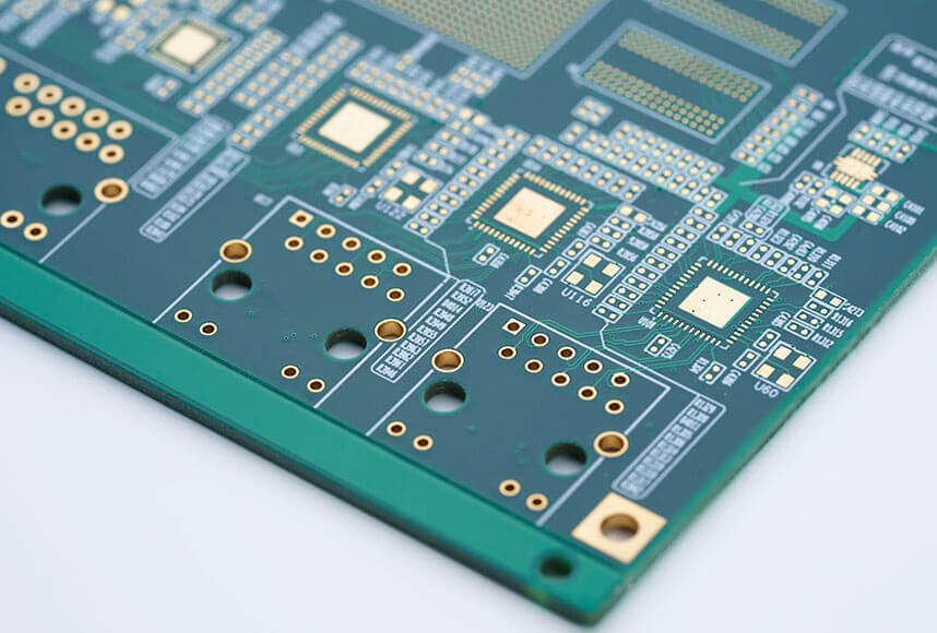
As an important trial production stage before mass PCB production, the prototype PCB fabrication has an important guiding significance for testing the function of new products. Prototype PCB fabrication can identify product design defects in the early stage, verify product function, and avoid batch scrap. PCB prototyping production in this stage needs rapid turnover, so as to shorten the development cycle of product iteration. This paper introduces the advantages of prototype PCB production and the high difficulty and complex PCB prototype production advantages of KKPCB.
In order to correct errors and defects and make the product have perfect functions, we must test the product in advance. The same for PCB. Before the printed circuit board is put into use, it must be ensured that it meets the standard and quality. In fact, despite the best efforts of designers and engineers, small, invisible errors can threaten the function and goal of the final PCB. If you don’t solve these problems, they become expensive and useless.
Before moving into more complex designs, they usually order multiple PCB prototypes runs to test the redesign or test a single function. This enables them to identify elements that need to be corrected early in the process. The earlier these problems are discovered, the lower the cost.
PCB Prototype: also known as a printed circuit board or prototype circuit board, PCB prototype board is widely used, almost all electronic products need PCB prototype and PCB prototype assembly, which leads to the growth of PCB prototype company.
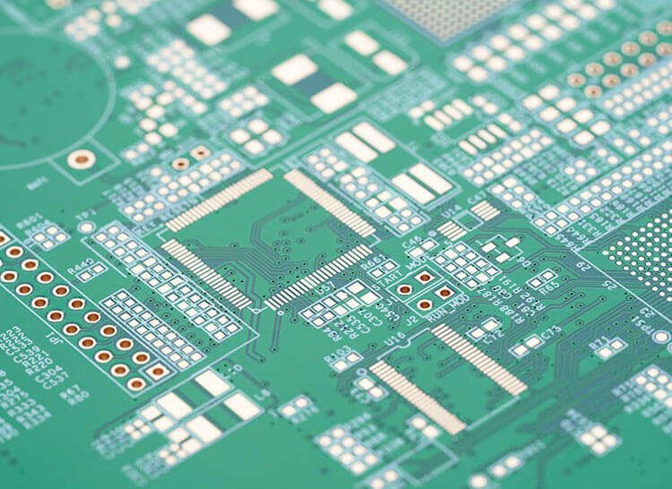
The PCB prototype is developed as a sample of a real PCB to test the design and ideas for an early understanding of the product. PCB modification design needs certain functions. All functions of PCB design are tested by PCB prototype. We use different types and designs of PCB prototypes to test different functions of PCB. Developers can use multi-functional PCB at all stages of the program. This depends on the size of the PCB hole and the thickness of the board.
So why use PCB prototypes instead of standard production runs? This may seem like an extra step, but in the long run, it can save you time and money and produce a better end product.
1. You may go through many design iterations when developing a new PCB-based design. You need to be able to test new designs quickly so that production can be completed in time, as a lengthy design process can lead to loss of revenue. The rapid speed of our prototyping services, combined with testing designs before production runs, can minimize wasted project expenditures and maximize your investment.
Standard production operations will also increase rapidly in terms of costs. The earlier you discover design defects or inefficiencies in a PCB design, the lower the cost of solving the problem. If you don’t use prototype boards to test your design, you may have problems later in the production run – that is, after you’ve invested a lot of money into producing standard PCBs. Our are also suitable for small volume production.
2. Engineers also often use prototype PCBs to test a single function of more complex products containing multiple PCBs. Before adding the next level of functionality, they will order prototypes that perform the most basic functions. If you don’t test the features separately, you may encounter performance problems in subsequent processes, and not sure which board caused the problem. Through the prototype design of each function step by step, a lot of time and resources can be saved.
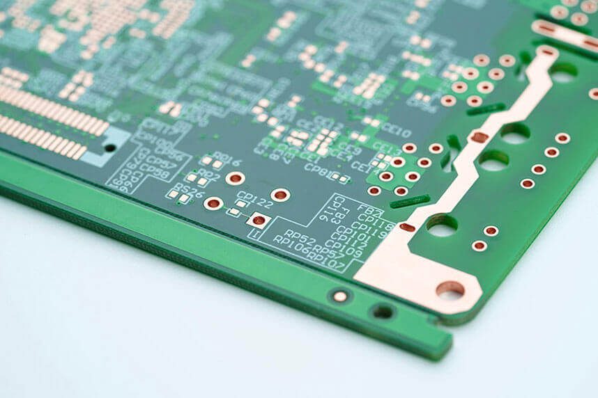
Although prototype PCBs do not allow manufacturing tolerances to be as high as those for standard production runs, they still accurately describe how the final PCB-based solution works. Once you have fully validated your design through the prototype board, you can continue with the standard production run, which has tighter manufacturing tolerances, can handle more functions, and can contain a larger order volume.
As part of our standard production products, we provide DFM to help identify any problems that may affect manufacturing. If we find any potential problems, we will contact you to develop the necessary solutions.
If you are developing new products or redesigning them, you may benefit from our prototype PCB production services. Before you invest a lot of time and money into a project, it will help you discover any potential problems or changes you may want to make to your design. This will raise the bottom line of your project, resulting in a higher quality end product and contributing to its overall success.
So choosing to order PCB prototypes instead of going directly to standard production runs provides many advantages. In almost any case involving new or updated design, PCB prototype design can prove to be beneficial. The advantages of using our PCB prototyping services include:
Fast turn around time
We can produce PCB prototypes faster than standard production PCB. We can complete the prototype order in just two days. Our standard production board takes 3 to 18 days to build, while our prototype takes only 2 to 5 days to build.
Early detection of defects
Prototyping enables you to catch design defects early in the product development process before you invest too much time and money into problem design. Engineering changes early in the process will avoid a number of potential problems.
Ability to test components individually
It is useful to test different components individually for complex project components involving multiple PCB-based projects. By validating each component individually, you can identify any problems that may occur. Without this, it’s hard to determine where the problem lies.
Accurate representation of standard PCB performance
High-quality PCB prototypes can accurately represent final production mode components. Although the tolerances are low, they still give you an idea of what you expect when you start a standard production run.
Efficient project completion
Use PCB prototypes to identify and correct design defects early, and quickly identify components that need to be adjusted. Failure to do so may significantly extend the time frame of the project, which may result in loss of revenue and customer dissatisfaction.
Reduce overall costs
By helping you find problems faster, it enables you to fix them before you invest in large volume standard production runs. By identifying problems in simpler product versions, you can redesign simpler components without having to build the entire project, which is more expensive.
Improved end products
PCB prototype design helps focus on improving each PCB and component to achieve a higher quality design. It can also help you avoid any undetected faults that may occur in the final product and cause more serious problems.
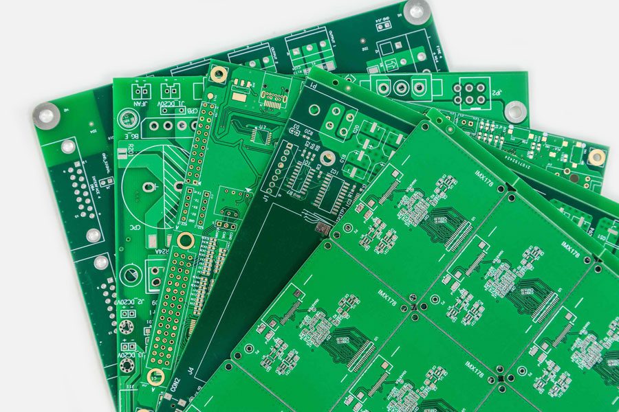
The benefits provided by PCB prototypes are used in most new or revised PCB designs. Once you have verified the functionality that prototypes must provide for the project, you can continue with the standard PCB production run.
Printed circuit boards that connect components through a variety of related circuits are the core of many different electronic devices we use every day. They have many different variants that enable them to function in a variety of situations. PCB is an integral part of electronic products used in almost all industries. You can find them in consumer electronics, medical equipment, auto parts, industrial equipment, lighting technology, aerospace equipment, etc.
As people continue to innovate and create more new electronic equipment, PCB becomes more common. It is in the development of these new products that the prototype PCB is the most useful.
When one of the following situations is involved, prototype design and manufacturing should be considered:
New products – any time your project involves developing a new product, you may not be able to detect any existing problems without prototype design, which can lead to more serious problems or more difficult to fix, enabling you to quickly and economically identify any factors that need to be adjusted.
Quality and design testing – if you want to do quality testing or design review, you should order a PCB prototype. A shorter build time will allow you to start reviewing or testing faster and will lower your overall costs. The PCB prototype will give you an accurate understanding of the performance of the final product.
Complex components – if your project contains multiple PCB-based components, use a PCB prototype. More components may mean more functionality, but more potential failures. Prototyping is particularly useful for these more complex projects because it helps quickly identify which component is not performing correctly. By ordering one PCB at a time, you can spend less time testing and correcting problems and save money.
At KKPCB, we provide a one-stop service for all your PCB prototype design and standard production requirements. We can complete every part of the prototyping process – including component procurement, manufacturing, assembly, and quality control. This way you don’t have to work with multiple PCB vendors to make the process more efficient and economical.
Time is crucial in today’s fast-growing industrial life, so it is necessary to follow this factor to save valuable resources. In PCB manufacturing, PCB with a fast turnaround is needed. In the process of quickly starting PCB, ensure that customers get the product within the specified time. A time frame is needed for this. Rapid production of PCB is undoubtedly very important to customers.
PCB manufacturing is a long process. It will take a few days to develop it. The quick turn PCB reduces the waiting time of PCB shoppers.
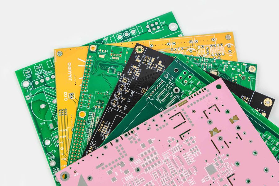
The key point of a rapid manufacturing PCB prototype is to carry out rapid PCB assembly before the final PCB product is complete. In a short time, PCB manufacturing becomes simple and fast. The quick start prototype PCB provides some core solutions for PCB shoppers.
KKPCB is a professional PCB prototype manufacturer. We spend a lot of time and energy updating our production process and technology and strive to provide the best quality PCB prototype service. We mainly produce single board and double board rapid prototyping, multilayer board, aluminum PCB, metal PCB, HDI board, and high-frequency PCB. Most importantly, we provide PCB assembly and component procurement to provide customers with one-to-one best PCB prototype service.
The production process of multilayer PCBs (Printed Circuit Boards) involves several sequential steps, each crucial for ensuring the quality and functionality of the final PCB.
Design Verification:
Error Detection and Correction:
Performance Testing:
Validation and Certification:
PCB Prototyping Process
Design Preparation:
Material Selection:
Fabrication:
Assembly:
Testing and Validation:
Iteration and Refinement:
Risk Reduction:
Cost Savings:
Time Efficiency:
Market Readiness:
When producing PCB prototypes, several surface treatment processes are commonly used to protect the exposed copper surfaces, enhance solderability, and ensure reliable electrical performance. Here are the primary surface treatment processes:
1. Hot Air Solder Leveling (HASL)
2. Electroless Nickel Immersion Gold (ENIG)
3. Organic Solderability Preservative (OSP)
4. Immersion Tin
5. Immersion Silver
6. Gold Finger
7. Hard Gold (Electrolytic Gold)
8. Electroless Nickel Electroless Palladium Immersion Gold (ENEPIG)
Choosing the appropriate surface treatment for a PCB prototype depends on several factors, including the specific application, environmental considerations, reliability requirements, and cost constraints. Each surface treatment has its own set of advantages and is selected based on the needs of the final product.
Testing PCB prototypes is a critical step to ensure that the design is functional, reliable, and free of defects before moving to mass production. Here are several methods used to test PCB prototypes:
1. Visual Inspection
2. Electrical Testing
3. Functional Testing
4. Environmental Testing
5. Signal Integrity Testing
6. X-ray Inspection
7. Software Testing
8. Burn-In Testing
9. Electromagnetic Compatibility (EMC) Testing
Testing PCB prototypes involves a combination of visual, electrical, functional, environmental, and specialized tests to ensure the board meets all design specifications and performance requirements. The specific tests chosen depend on the PCB's intended application, complexity, and reliability requirements. By thoroughly testing prototypes, engineers can identify and resolve issues early, ensuring a higher-quality product in mass production.
The materials used for PCB prototypes are similar to those used for regular PCBs, but the selection may be tailored to meet specific prototyping needs such as speed, flexibility, and cost-efficiency. Here are the primary materials used in PCB prototypes:
1. Substrate Materials (Base Materials)
FR-4 (Flame Retardant 4):
Polyimide:
PTFE (Polytetrafluoroethylene):
Metal Core (MCPCB):
2. Copper Foil
Standard Copper Foil:
High-Density Copper Foil:
3. Prepreg (Pre-impregnated Material)
4. Solder Mask
Epoxy Liquid Solder Mask:
LPI (Liquid Photoimageable) Solder Mask:
5. Surface Finishes
HASL (Hot Air Solder Leveling):
ENIG (Electroless Nickel Immersion Gold):
OSP (Organic Solderability Preservative):
6. Silkscreen
7. Adhesives
8. Other Specialized Materials
Rogers Material:
Ceramic Substrates:
Selecting the appropriate materials for a PCB prototype depends on the specific requirements of the design, including electrical performance, thermal management, mechanical strength, and cost considerations.
PCB prototypes are used across a wide range of industries to develop, test, and refine electronic products before full-scale production. Here are some key industries that heavily rely on PCB prototypes:
1. Consumer Electronics
2. Automotive
3. Telecommunications
4. Medical Devices
5. Aerospace and Defense
6. Industrial and Automation
7. Renewable Energy
8. Computing and Data Centers
9. IoT (Internet of Things)
10. Research and Development
11. Lighting
12. Agriculture
13. Test and Measurement
PCB prototypes play a critical role in the development and testing of electronic products across these diverse industries. They help engineers and designers validate designs, identify and resolve issues, and ensure that the final products meet industry standards and performance requirements.
A PCB prototype differs from a regular (production) PCB in several key aspects, primarily related to their purpose, manufacturing processes, and use cases. Here are the main differences:
1. Purpose
PCB Prototype:
Regular PCB:
2. Manufacturing Process
PCB Prototype:
Regular PCB:
3. Quality and Testing
PCB Prototype:
Regular PCB:
4. Design and Features
PCB Prototype:
Regular PCB:
5. Production Volume
PCB Prototype:
Regular PCB:
6. Cost Considerations
PCB Prototype:
Regular PCB:
In summary, PCB prototypes are essential for design validation, testing, and iteration, allowing engineers to refine their designs before committing to large-scale production. Regular PCBs, on the other hand, are the final product ready for use in commercial applications, produced with a focus on consistency, reliability, and cost-effectiveness.
Choosing a professional PCB prototype manufacturer is a critical decision that can significantly impact the quality, cost, and turnaround time of your project. Here are some key factors to consider when selecting a PCB prototype manufacturer:
1. Experience and Expertise
2. Capabilities and Services
3. Quality Standards
4. Turnaround Time
5. Cost and Pricing
6. Customer Service and Communication
7. Technical Capabilities
8. Material Selection
9. Reputation and Reviews
10. Geographical Location
11. Prototyping Flexibility
12. Post-Production Support
Steps to Choose a Manufacturer
By carefully considering these factors and following a structured selection process, you can choose a professional PCB prototype manufacturer that meets your specific needs and ensures the success of your project.