Pros and Cons of Copper Coating in PCB Design
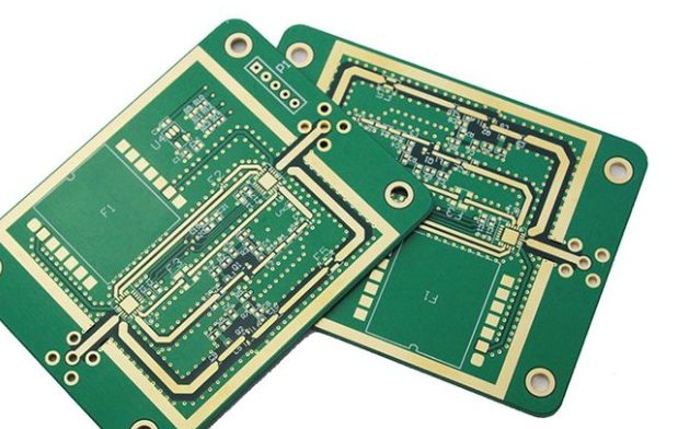
Copper coating, also known as copper filling, is an essential aspect of PCB design that plays a key role in reducing impedance, improving anti-interference capabilities, and enhancing the overall efficiency of power delivery. However, there are several factors to consider when applying copper coating, and the effectiveness depends on how well it is executed. Let’s explore the advantages and disadvantages of copper coating in PCB design.
Advantages of Copper Coating:
- Improved Grounding and Reduced Impedance: Copper coating reduces the impedance of the ground line, making it more effective at dissipating noise and electromagnetic interference (EMI). A better-grounded PCB design improves the overall performance of the circuit, particularly in high-frequency applications.
- Enhanced Anti-Interference Capabilities: Copper filling acts as a shield that helps reduce the impact of external interference, thus protecting sensitive components from noise and improving signal integrity.
- Better Power Supply Efficiency: Copper coating reduces the voltage drop across the PCB, improving the power supply efficiency and ensuring a more stable voltage supply to critical components.
- Reduced Loop Area: Copper filling helps minimize the loop area, which decreases the electromagnetic radiation and the susceptibility of the board to external electromagnetic fields. This is particularly beneficial in reducing EMI in sensitive circuits.
- Decreased PCB Warping: Filling open areas on the PCB with copper can help prevent board warping during the soldering process. By creating a more uniform thermal expansion, copper coating stabilizes the PCB, especially during wave soldering.
- Improved Heat Dissipation: Copper coating can also act as a heat sink, helping to dissipate heat generated by high-power components and ensuring that the board operates within safe temperature limits.
Disadvantages of Copper Coating:
- Potential for Board Warping or Bubbling: While copper coating can stabilize the PCB, if applied improperly, it can lead to board warping or even bubbling during the soldering process, especially in large areas of copper. To prevent this, grooves are often added to large copper sections to avoid the buildup of internal stresses.
- Potential Grounding Issues: If copper is not properly grounded, it can become a source of noise rather than a shield. Poor grounding may lead to unwanted noise propagation and EMI. Therefore, it’s crucial to ensure that copper areas are well connected to the PCB’s ground.
- Antenna Effect in High-Frequency Circuits: For high-frequency applications, large copper areas may inadvertently act as antennas, radiating noise and interfering with the circuit’s performance. The presence of poorly grounded copper can exacerbate this problem.
- Complexity in Grid Copper: While grid copper is effective for shielding, it can create complications at certain frequencies. If the electrical length of the grid lines matches the operating frequency of the circuit, it may cause interference, and the circuit could fail to work properly.
- Risk of Signal Interference: For high-frequency circuits, grid copper lines may not be ideal since their electrical length can lead to signal interference. Careful consideration of the operating frequency is necessary to avoid disrupting the circuit’s functionality.
Best Practices for Copper Coating:
- Use 0-ohm Resistors or Inductors for Ground Connections: When connecting different ground points, use 0-ohm resistors, magnetic beads, or inductors to maintain proper isolation.
- Copper Coating Around Crystal Oscillators: Surrounding crystal oscillators with copper coating and grounding the shell separately can help mitigate the high-frequency noise emissions from the oscillator.
- Avoid Dead Zones (Islands): Avoid leaving large areas of unconnected copper, known as “islands” or “dead zones.” These should be properly grounded to prevent them from becoming noise sources.
- Ground Wire Routing: Ensure that the ground wires are routed effectively before copper plating. Adding vias afterward is not a recommended practice, as it may not provide a solid ground connection.
- Avoid Sharp Corners: Sharp corners in PCB traces can act as antennas, radiating electromagnetic interference. It’s best to use smooth, rounded edges to minimize this effect.
- Separate Grounds for Digital and Analog Circuits: If there are multiple grounds (e.g., SGND, AGND, GND), each should be separately coated with copper, and the most important ground should be used as the reference. Analog and digital grounds should not be mixed to prevent interference.
- Avoid Copper Coating on Middle Layers of Multilayer Boards: Avoid applying copper coating to middle layers in multilayer boards unless the copper can be properly grounded. This can be difficult to achieve and may cause grounding issues.
- Proper Grounding for Metal Components: Ensure that metal components like heat sinks, reinforcement strips, and three-terminal regulators are properly grounded to maintain the overall stability of the PCB.
When applied correctly, copper coating offers more benefits than drawbacks, providing improved performance, noise reduction, and thermal management for PCBs. However, to achieve the best results, it’s crucial to carefully consider the design, including grounding, copper areas, and the specific requirements of high-frequency or low-frequency circuits. By paying attention to these details, designers can optimize the copper coating for better overall performance.

