Printed Circuit Board from design to production
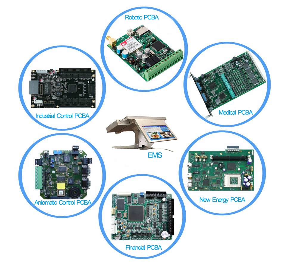
In today’s technology-driven world, the Printed Circuit Board (PCB) stands as a foundational component in electronic devices. From smartphones to complex medical equipment, PCBs are essential for ensuring reliable electrical connections and functionality. This article delves into the critical stages of PCB design, manufacturing, and final artwork, providing insights into the complexities and technicalities of creating effective circuit boards.
Understanding the Printed Circuit Board
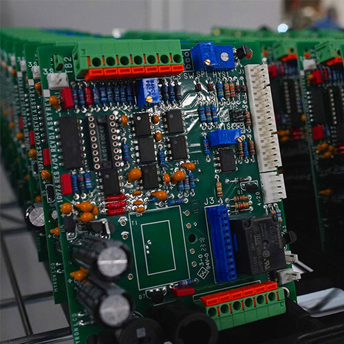
A Printed Circuit Board is a flat, rigid board that supports and connects electronic components through conductive pathways, known as traces. These traces are typically made from copper, which is applied to a dielectric substrate, often FR-4, a flame-resistant material composed of woven fiberglass and epoxy resin. The design process begins with a clear understanding of the board’s intended function, which dictates its specifications, layout, and component placement.
The Design Process
The PCB design process consists of several stages, beginning with schematic capture. During this phase, engineers use CAD software to create a detailed diagram that represents the electrical connections among components. This schematic serves as a blueprint for the PCB layout, defining how components like resistors, capacitors, and integrated circuits will interact.
Once the schematic is complete, the next step is to develop the physical layout of the Printed Circuit Board. This involves placing components on the board and routing the traces that will connect them. Designers must consider various factors, including trace width, spacing, and layer stacking, to ensure optimal electrical performance and reliability.
Library Development
A crucial aspect of the design process is the creation of a library of CAD parts. This library includes symbols for each component, simulation models, and footprints that outline how components will be placed on the PCB. By developing this library, designers streamline the layout process, allowing for quicker adjustments and ensuring that all components meet design specifications.
PCB Layout and Routing
The layout phase is where the theoretical aspects of design meet practical application. Engineers utilize PCB design software to transfer the schematic into a physical layout, placing components in an optimal configuration. This step is critical because it influences the board’s performance, manufacturability, and overall reliability.
Once components are positioned, designers route traces to connect them. This process involves careful consideration of signal integrity, electromagnetic interference (EMI), and thermal management. For high-speed applications, minimizing trace length and ensuring proper impedance is vital. Automated routing tools can assist in this phase, but manual adjustments are often necessary to optimize performance.
Manufacturing Process
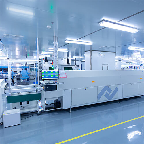
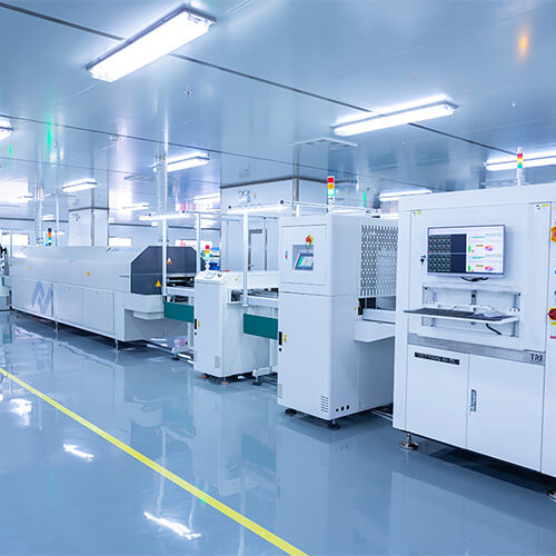
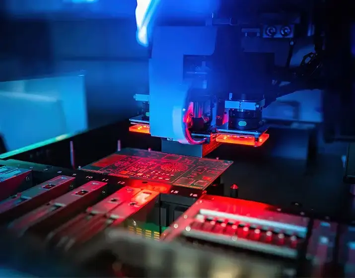
After the design is finalized, the Printed Circuit Board must undergo a manufacturing process. This includes several steps: etching the copper layers, applying solder mask, and printing silkscreen labels for identification. Each step requires precision to ensure that the final product meets quality standards.
The manufacturing stage also involves testing the PCB for functionality. Techniques such as Automated Optical Inspection (AOI) and Electrical Testing (E-Test) help identify defects before the board is assembled. This quality assurance process is critical, especially for Class 3 PCBs, which are used in applications where failure could have serious consequences.
Final Artwork and Assembly
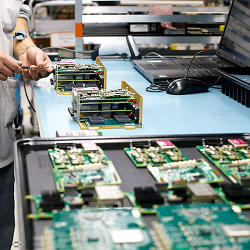
Once the PCB is fabricated and tested, the next step is assembly. Components are soldered onto the board using methods like Surface Mount Technology (SMT) or Through-Hole Technology (THT). The assembly process can vary based on the complexity of the design and the type of components used.
Finally, the Printed Circuit Board is subjected to a final inspection and testing phase to ensure it functions as intended. This might include functional tests, thermal cycling, and environmental stress testing to confirm reliability under various conditions.
Conclusion
The journey of a Printed Circuit Board from design to final artwork is intricate and multifaceted, involving detailed planning, technical expertise, and rigorous testing. As technology continues to advance, understanding the fundamentals of PCB design and manufacturing becomes increasingly important for engineers and manufacturers alike. By mastering these principles, professionals can create high-quality, reliable PCBs that are crucial for the performance of modern electronic devices.

