Practical Skills in High-Frequency PCB Design
In PCB design, achieving smaller, faster, and more cost-effective products is key. High-frequency PCB design presents unique challenges, especially at interconnection points, where electromagnetic properties must be carefully managed. This article focuses on practical skills for interconnection within the PCB board, providing valuable insights for engineers.
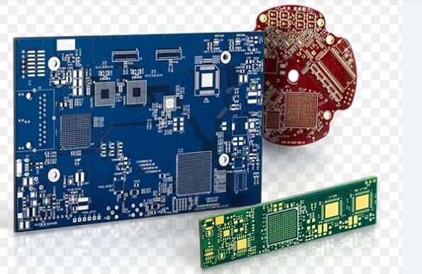
For high-frequency applications, consider the following PCB design skills:
- Use 45° Transmission Line Corners: Reduce return loss by ensuring transmission line corners are angled at 45°, which improves signal integrity.
- Choose High-Performance Insulating Materials: Use insulating circuit boards with well-controlled dielectric constants to effectively manage the electromagnetic fields between the material and adjacent wiring.
- Precision Etching in PCB Design: Define strict etching specifications, such as maintaining a total line width error of +/- 0.0007 inches. Proper control of wiring geometry and sidewall plating is crucial for reducing skin effect issues at microwave frequencies.
- Avoid Leaded Components: Leads introduce tap inductance, so opt for surface-mount components to minimize high-frequency interference.
- Minimize Via-Induced Inductance: Avoid using through-hole (PTH) vias on high-frequency-sensitive layers. Vias connecting multiple layers can introduce unwanted lead inductance, affecting the performance of other layers.
- Add Ground Layers: Ensure ample ground layers are connected using via holes to counteract the effects of 3D electromagnetic fields on the board.
- Use Non-Electrolytic Nickel or Immersion Gold Plating: Avoid the HASL (Hot Air Solder Leveling) process, as immersion gold or nickel plating provides better skin effect for high-frequency currents. It also offers better solderability and reduces environmental impact.
- Use Solder Dams Instead of Full Solder Masks: Full solder masks introduce unpredictability in thickness and insulation properties, affecting electromagnetic energy. Use solder dams instead to improve microstrip design performance.
Following these practical tips for high-frequency PCB design helps in optimizing interconnections within the board. Techniques such as using 45° transmission lines, precision etching, and non-leaded components will significantly enhance circuit performance. Familiarizing yourself with these methods makes designs like back-copper coplanar microstrip layouts both economical and efficient.


