PCB special process classification
The special processes of PCB include but are not limited to the following categories:
1.Ultra-thin board and ultra-thick board: Ultra-thin board refers to a PCB with a thickness smaller than the standard thickness, while ultra-thick board refers to a PCB with a thickness greater than the standard thickness. These processes are often used in specific electronic products, such as thin and light electronic products (such as smartphones, tablets) or high-power electronic equipment (such as power modules, motor drivers).
2.Impedance board: The impedance board has a preset impedance value and is used to control the flow of current on the PCB to optimize circuit performance.
3.Carbon oil and gold fingers: Carbon oil is a coating used to increase the wear resistance and conductivity of PCB, while gold fingers are the connection parts of PCB coated with gold coating to provide high-quality electricity. connect.
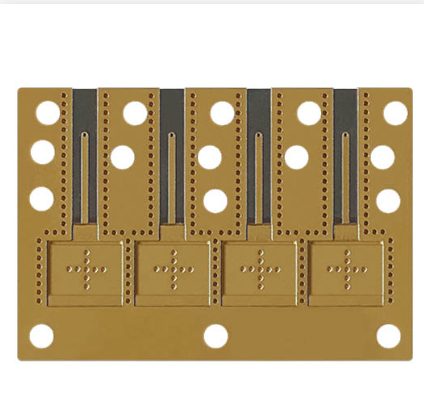
4.Blind and buried vias: Blind vias are holes that are only visible on one of the top or bottom layers; buried vias are via holes on the inner layer, and the upper and lower sides of the hole are on the inner layer of the board. These processes can improve the signal quality and overall performance of the PCB.
5.Thick copper plate: A layer of copper foil is bonded to the outer layer of FR-4. When the finished copper thickness is >2oz, it is defined as a thick copper plate. This process can improve the heat dissipation capacity and voltage resistance of the PCB.
6.Multi-layer special laminated structure: The laminated structure is an important factor affecting the EMC performance of the PCB board, and is also an important means of suppressing electromagnetic interference.
7.Electroplating nickel gold/gold finger: Electroplating nickel gold refers to making gold particles adhere to the PCB board through electroplating. Because of its strong adhesion, it is called hard gold; using this process, the hardness and resistance of the PCB can be greatly increased. Abrasive, effectively prevents the diffusion of copper and other metals, and adapts to the requirements of hot pressure welding and brazing.
8.Nickel-plated gold: In PCB proofing, chemical methods are used to deposit a layer of nickel, palladium and gold on the surface of the copper layer of the printed circuit. It is a non-selective surface processing technology.
9.Special-shaped holes: PCB production often encounters the production of non-circular holes, which are called special-shaped holes. Including figure-8 holes, diamond holes, square holes, zigzag holes, etc., which are mainly divided into two types: copper in the hole (PTH) and no copper in the hole (NPTH).
These special processes can improve the performance, appearance, and functionality of PCBs, but they also increase design and manufacturing costs.
KKPCB conducts research on special processing technologies such as ordinary double-sided boards, thick copper circuit boards, high-frequency circuit boards, HDI circuit boards, rigid-flexible circuit boards, FPC flexible boards, buried blind hole circuit boards, and IC carrier boards. Provides PCB design, PCB layout, PCB prototyping and PCB assembly services.

