


PCB Routing: Best Practices for Ensuring Signal Integrity and Performance
Printed Circuit Board (PCB) routing is a critical aspect of electronic design, ensuring that electrical signals are transmitted efficiently and reliably between components. Proper routing minimizes interference, maintains signal integrity, and meets design requirements such as impedance control and thermal management. This article outlines the best practices for PCB routing, focusing on optimizing performance and ensuring signal integrity.
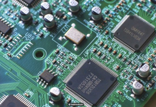
Understanding PCB Traces
PCB traces are conductive pathways made of copper that carry electrical signals between components such as integrated circuits (ICs), resistors, and capacitors. These traces are formed by coating a copper-clad board with a photosensitive material, exposing it to ultraviolet light through a mask to define the circuit pattern, and then etching away the unexposed copper. Proper routing of these traces is essential for the circuit’s functionality, as they provide the path for electrical current flow.
PCB Routing Best Practices
1. Planning and Strategy
- Component Placement: Plan the placement of components and the overall routing strategy to maximize performance and minimize interference. Group related components together to reduce trace lengths and simplify routing.
- Critical Signals: Route critical signals (e.g., high-speed or sensitive signals) first to ensure they have the shortest and most direct path on the PCB.
2. Trace Design
- Trace Width: Choose trace width based on current-carrying capacity and impedance requirements. Ensure consistent trace width to maintain controlled impedance and prevent signal reflections.
- Trace Length: Minimize trace length to reduce signal propagation delay and attenuation. For high-speed signals, shorter traces help maintain signal integrity.
- Avoid Sharp Corners: Use 45-degree angles or curved traces instead of sharp corners or right angles to reduce electromagnetic interference (EMI) and signal reflections.
3. Signal Integrity Considerations
- Impedance Control: Maintain consistent trace impedance by controlling trace width, thickness, and the dielectric constant of the PCB material. Use impedance calculators or field solvers to design traces with the desired impedance.
- Crosstalk Mitigation: Separate high-speed signal lines to minimize electromagnetic coupling (crosstalk). Keep analog and digital signals apart to reduce interference.
- Trace Length Matching: For parallel data buses or differential pairs, match trace lengths within specified tolerances to prevent skew and maintain signal timing integrity.
4. Layer Stackup Design
- Ground and Power Planes: Use dedicated ground and power planes to provide low-impedance return paths and reduce EMI. Ensure high-speed signals have a clear return path to complete their circuit loop.
- Controlled Impedance Layers: Design the PCB layer stackup with signal integrity in mind. High-speed signals may require specific layer arrangements and materials for controlled impedance routing.
5. Noise Management
- Sensitive Signals: Route sensitive analog signals away from noisy digital components to minimize interference and improve signal integrity.
- Signal Termination: Use termination techniques such as series resistors or shunt terminations to minimize signal reflections and ringing. The termination method depends on the signal type and transmission line characteristics.
6. Testing and Validation
- Signal Integrity Analysis: Use simulation tools to analyze signal behavior and predict issues such as reflections, crosstalk, and impedance mismatches. Optimize the design before manufacturing.
- Prototype Testing: Test PCB designs using prototypes to identify and resolve any issues before full-scale production.
Key Considerations for Signal Integrity
- Signal Requirements: Understand the electrical characteristics of the signal, including frequency, rise/fall times, and voltage levels. This information guides decisions about trace geometry, impedance, and routing topology.
- Return Path: Ensure high-speed signals have a low-impedance return path, typically provided by a ground plane or adjacent ground traces.
- Differential Pairs: Route differential pairs with consistent spacing and parallelism to minimize common-mode noise rejection.
- Thermal Management: Consider thermal dissipation when routing high-current traces. Use wider traces or copper pours to manage heat effectively.
Proper PCB routing is essential for ensuring signal integrity, minimizing errors, and maximizing system reliability. By following best practices such as optimizing trace width and length, controlling impedance, mitigating crosstalk, and using ground planes, designers can create high-performance PCBs that meet design requirements. Additionally, leveraging simulation tools and prototype testing helps identify and resolve potential issues early in the design process, ensuring a robust and reliable final product.