High-Speed PCB Design Guide 8: PCB Reliability Design
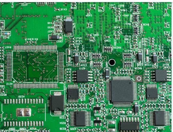
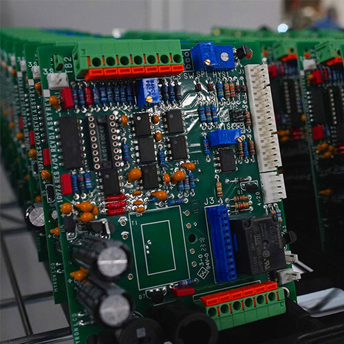
Printed circuit boards (PCBs) remain the backbone of electronic assembly across various systems. Even with perfectly designed schematics, poor PCB design can significantly compromise reliability. For instance, closely spaced thin parallel lines on a PCB can cause signal waveform delays and reflected noise at transmission line terminals. This guide outlines essential considerations for designing reliable PCBs.
1. Ground Wire Design
Effective grounding is critical for controlling interference. Proper grounding methods can resolve most interference problems. Ground structures typically include:
- System ground
- Chassis ground (shielded ground)
- Digital ground (logic ground)
- Analog ground
Key Points in Ground Wire Design:
- Single-point vs. Multi-point Grounding
- For low-frequency circuits (<1MHz), single-point grounding minimizes loop interference.
- For high-frequency circuits (>10MHz), multi-point grounding reduces ground impedance.
- For frequencies between 1–10MHz, ground wire length should not exceed 1/20 of the wavelength; otherwise, multi-point grounding is recommended.
- Separate Digital and Analog Grounds
- Keep high-speed digital circuits and linear analog circuits apart.
- Ground each circuit type separately and connect them to the power ground.
- Thick Ground Wires
- Thin ground wires increase impedance and reduce noise immunity. Ground wire width should ideally exceed 3mm.
- Closed-loop Grounding
- A closed-loop ground structure improves noise immunity by reducing potential differences across ground junctions.
2. Electromagnetic Compatibility (EMC) Design
EMC ensures electronic systems operate reliably without causing or being affected by electromagnetic interference.
Strategies for EMC Optimization:
- Wire Width
- Wider wires reduce inductance. Signal lines carrying high transient currents (e.g., clock lines) should be short and wide.
- Correct Routing
- Use a tic-tac-toe wiring structure: horizontal on one layer, vertical on the other, connected by vias. Avoid long parallel traces and reduce cross-talk by inserting grounded lines.
- Minimize Discontinuities
- Avoid sudden width changes, sharp corners, and looped routing.
- Clock Signal Management
- Route clock signals near ground loops to reduce radiation.
- Signal Bus Optimization
- Add ground lines between data bus traces. Place drivers close to connectors and ensure high-speed devices are well-separated from sensitive components.

3. Decoupling Capacitor Configuration
Decoupling capacitors suppress noise caused by load changes. Proper configuration enhances PCB reliability:
- Electrolytic Capacitors
- Add 10–100µF capacitors at power inputs. Larger values (>100µF) provide better anti-interference.
- Chip-Level Capacitors
- Use 0.01µF ceramic capacitors for each IC or 1–10µF tantalum capacitors for every 4–10 ICs in tight spaces.
- Connection Guidelines
- Place decoupling capacitors near power (Vcc) and ground (GND) terminals with minimal lead length, especially for high-frequency components.
4. PCB Size and Component Layout
Size Optimization:
- Large PCBs increase impedance and noise susceptibility.
- Small PCBs suffer from heat dissipation issues and adjacent line interference.
Layout Considerations:
- Position related components close together for minimal noise.
- Separate high-heat, noise-sensitive, and low-current devices.
- For heat dissipation, mount PCBs vertically, with a minimum gap of 2cm between boards.
5. Thermal Design
Key Thermal Management Principles:
- Arrange components based on heat generation and resistance.
- Place high-power devices near PCB edges to shorten heat transfer paths.
- Avoid positioning temperature-sensitive devices above heat sources.
6. Interference Suppression Strategies
Grounding Techniques:
- Signal Grounding
- Use floating, single-point, or multi-point grounding based on frequency and application needs.
- Equipment Grounding
- Connect chassis to earth for safety, charge dissipation, and stability.
Shielding Methods:
- Electric Field Shielding
- Use grounded metal shields between high- and low-potential areas.
- Magnetic Field Shielding
- Employ high-permeability materials to shunt magnetic fields.
- Electromagnetic Shielding
- Combine surface reflection and material absorption for optimal EMI reduction.
7. Product Electromagnetic Compatibility
PCB EMC Best Practices:
- Separate digital and analog ground planes.
- Minimize current loops and maintain consistent line widths.
- Use decoupling at power line inputs to suppress interference.
Switching Power Supply EMC:
- Use power filters and insulating gaskets to suppress grid disturbances.
- Minimize loop areas and “trim” switching waveforms to reduce radiated noise.
Reliability in PCB design hinges on tailored approaches for grounding, EMC, thermal management, and interference suppression. Adhering to these principles enhances system performance and longevity, reducing failure rates. Practical application of these guidelines, customized for specific circuits, ensures robust, interference-resistant PCBs.


