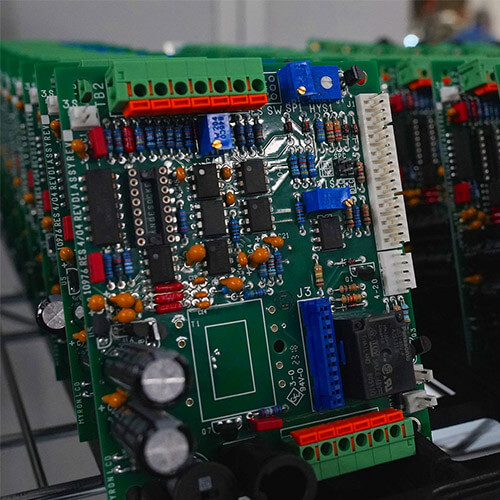
PCB Production Process: Subtractive and Additive Methods
Printed Circuit Boards (PCBs) are the foundation of most electronic devices. The PCB production process can be categorized into subtractive methods and additive methods. Currently, the most commonly used industrial method is the copper foil etching process, a subtractive method.
1. PCB Substrate Processing
The PCB substrate is typically classified based on its insulating material. Popular raw materials include bakelite, fiberglass boards, and various plastic boards. Most manufacturers use a combination of glass fiber, non-woven material, and epoxy resin, which is pressed together with copper foil to form the prepreg.
Common PCB substrates for high-performance applications like Xgs game console circuit design include:
- FR-1: Phenolic cotton paper (Bakelite)
- FR-4: Woven glass, epoxy resin
- CEM-1, CEM-3: Cotton paper/glass cloth with epoxy resin
- AIN: Aluminum nitride
- SIC: Silicon carbide
2. Metal Coating in PCB Production
The metal coating on a PCB connects electronic components and facilitates soldering. The choice of metal directly impacts production costs, solderability, and circuit performance.
Common metal coatings include:
- Copper
- Tin (5-15 μm)
- Lead-tin alloy (5-25 μm, tin content around 63%)
- Gold and Silver (typically used on interfaces)
3. PCB Circuit Design
Designing a PCB involves transforming a circuit schematic into a layout. This includes arranging components, creating metal connections, adding through holes, and designing for electromagnetic protection and heat dissipation. Complex PCB designs often require CAD software like OrCAD, Altium Designer, and CAM350.
4. PCB Manufacturing Process: Subtractive and Additive Methods
Subtractive Method
The subtractive method removes unwanted metal areas on a copper-clad board, leaving behind the necessary circuits. Techniques include:
- Screen printing
- Photosensitive board exposure
- Engraving (CNC milling or laser)
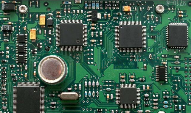
Additive Method
In the additive process, a thin copper substrate is covered with a photoresist, exposed to UV light, and developed. Electroplating is then used to increase copper thickness in the desired circuit areas, followed by removing the photoresist and etching away excess copper.
5. Functional Testing of PCBs
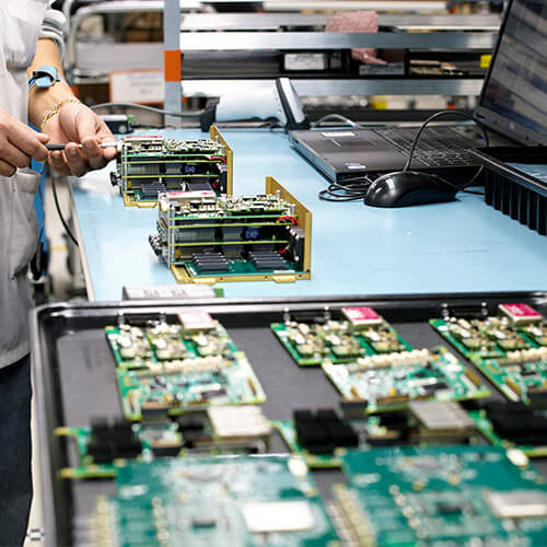
As PCBs become more dense with higher bus speeds and analog RF circuits, functional testing becomes essential. Test engineers must balance automated testing and manual probing based on geographic factors (e.g., labor costs in Thailand vs. California). Accurate testing depends on clear marking of test points and ensuring operator safety during probing.
6. Automatic Probing for PCB Testing
In scenarios where manual probing is impractical, automatic probing systems can reduce errors, minimize the risk of short circuits, and improve test speeds. Factors like UUT size, probe positioning accuracy, and compatibility with the SMEMA standard for online environments must be considered.
7. Boundary Scan Testing
Boundary scan technology allows for more efficient testing of digital circuits by embedding additional pins and lines on the circuit, enabling diagnostics with minimal probing. This technique is also useful for programming flash memory and PLDs on the PCB.
8. PCB Layout Design Considerations
When designing a PCB, especially single-sided or double-sided boards, careful attention must be paid to:
- Component layout
- Plated through-hole (PTH) usage
- Component mounting area (C/S ratio)
- Signal routing efficiency
9. PCB Production Checklist
Before finalizing the PCB design, review the following:
- Has the circuit been properly analyzed for signal flow?
- Are the key leads short or isolated?
- Is the circuit shielded where necessary?
- Are the grid patterns optimally used?
- Are the wire width and spacing adequate for signal integrity?
- Are jumpers minimized, and letters legible after assembly?
10. Technical Challenges in PCB Production
PCB production challenges include optimizing design for manufacturability and ensuring high-quality automated testing for mass production. Attention to probe size, test point clarity, and operator safety are crucial for ensuring accurate and reliable PCB performance.

