One-stop PCB Manufacturing and PCB Assembly solutions Manufacturer
- Mon - Sat: 8.00 am - 7.00 pm
- sales@kkpcb.com
One-stop PCB Manufacturing and PCB Assembly solutions Manufacturer
Over 10 years we help companies reach their financial and branding goals. Engitech is a values-driven technology agency dedicated.
411 University St, Seattle, USA
engitech@oceanthemes.net
+1 -800-456-478-23
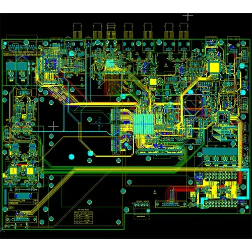
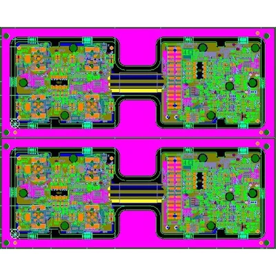
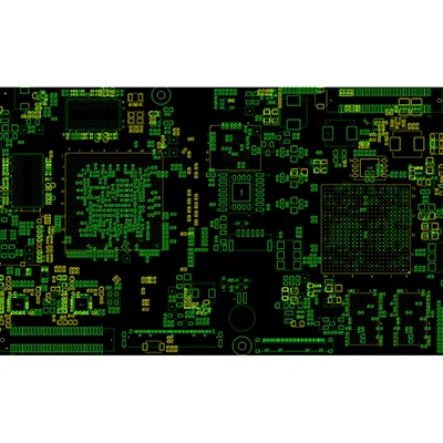
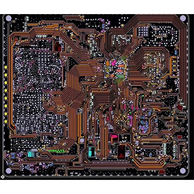
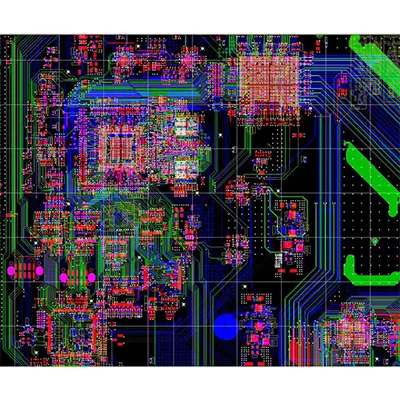
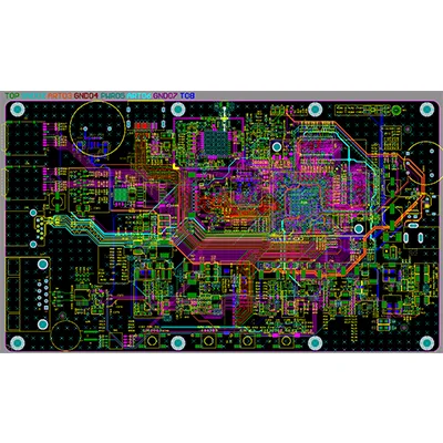
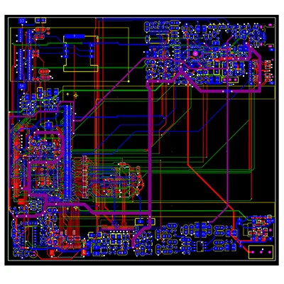
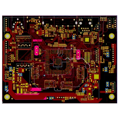
As a leading PCB manufacturer, members of our printed circuit board (PCB) design service team are practical partners working with you on every project and can help you achieve your goals at any time. They can complement your engineering expertise, which helps speed up time to market, reduce the time from concept to production, and ensure that quality is integrated into the manufacturing process to maximize your profits.
51% of smartphone users have discovered a new company or product.
Move your SaaS products to mobile, Companies with a professional mobile.
Develop a custom mobile app to thrive in a mobile market worth over $100.
80% of time users spend in social mediafrom their mobile devices.
65% of sales representatives have achieved their quotas by adopting.
We provide top-tier mobile app development services for brokers.
Maximum design layers of PCB: 64 layers
Maximum number of PINs: 110000+
Maximum connections: 78000+
Minimum line width: 2 mil
Minimum line spacing: 2 mil
Minimum through hole: 6mil (4mil laser hole)
Maximum BGA quantity: 120+
Minimum BGA PIN spacing: 0.3mm
Maximum number of BGA PINs: 8371
Maximum speed signal: 112G-PAM4
1. PCB libraries accumulated over 10 years
2. Database data query system, 95% BOM automatic matching
3. All verified through mass production
4. EDA tools
5. Database construction checklist
6. IPC7351 specification
1. Netlist import and export
2. Interconversion of PCB libraries for different EDA software
3. Customized project library building service
4. Creating custom schematic symbols
5. Customize and maintain customer-exclusive libraries
1. PCI, local bus multi-load topology scheme
2. Memory design (DDR1/2/3/4)
SERDES design (PCIE, SATA, XAUI...)
3. RapidIO 10G BASE-KR, SFI, XFI, CEI-6G, CEI-28G...)
4. High speed backplane design (CPCI, ATCA, VPX...)
1. Server and Industrial Control
2. Communication equipment
3. Consumer
4. Security
5. Monitoring
6. IoT Products
7. Automotive electronics
A printed circuit board layout design is a very important element that you should consider in designing electronic products.
In many cases, a design engineer is responsible for designing the electronic circuit.
A printed circuit board layout designer is responsible for taking the PCB layout and design from the given schematic.

The PCB layout and design is a special skill that requires you to have knowledge of the basic software.
The type of software that you should have knowledge of is inclusive of the CAD system plus a variety of techniques.
The standards that you will use will ensure a successful transfer of the circuit board to the printed circuit board.
It will also ensure success in the process of manufacturing the printed circuit board in a manufacturing environment.
For a successful manufacture of a printed circuit board, you should have guidelines that you will follow in the process.
There are experts who have experience in the system and are able to design a layout without a guideline.
When it comes to the process of making a printed circuit board design, different software is available for use.
It is important to choose software that many people in the designing industry prefer to use.
Remember, this is an important factor to consider when doing team designs as the software will enhance the skill of engineers.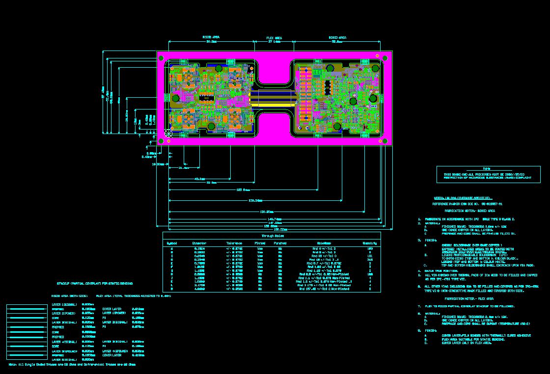
The printed circuit board layout and design software that many people use include Xpedition, PADS, Altium and Cadence Allegro.
The software is suitable for the job of designing the PCB layouts but some do better jobs than others.
The programs that you will use range from simple products to products that have very high sophistication.
There are quite a number of printed circuit board designs that you can choose from depending on the application.
Continue reading and find out more about the most common types of PCB designs that you can use.
A flex PCB design is a type of printed circuit board that is able to bend at different angles.
The material that you will use in making the flex PCB should have the ability to bend round different corners.
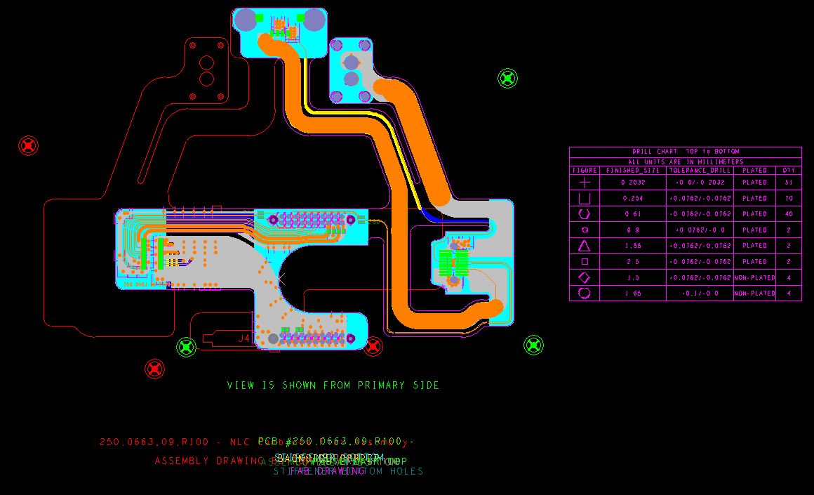
The main materials in a flex PCB design are copper and flexible substrate materials put together using pressure, heat and adhesives.
The substrate that many manufacturers use is the polyimide which is a flexible and strong thermosetting polymer.
Examples of polyimides that you can use are Kapton, Apical, VTEC PI, UPILEX, Kaptrex and Norton TH.
It is, therefore, a pattern of different conductors on an insulating film that is flexible
As the name suggests, it is a printed circuit board with a rigid circuit and a flexible circuit operating together.
The rigid-flex design is important as it has the benefits of the rigid and flexible circuits.
The rigid circuit carries most of the components of the PCB while the flexible area acts as the connections.

The flexible area is meant to save weight and space and is components of portable devices such as cell phones.
It also helps in the reduction of packaging complexity as it eliminates the need of doing interconnect wirings.
A multilayer PCB is a design of a printed circuit board that has three or more layers.
It has more than three layers of conductors which you will find at the centre of the material.
It is an essential component of aerospace printed circuit boards and critical crosstalk levels equipment.
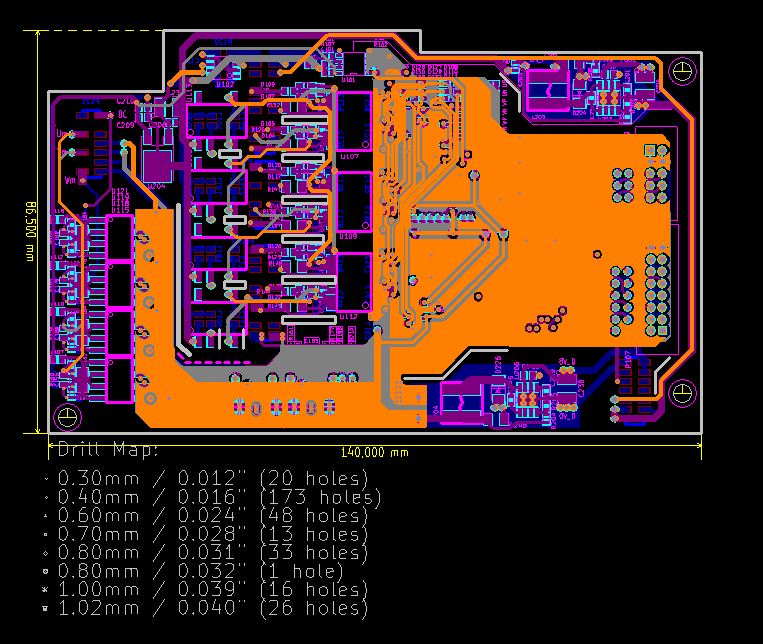
You can also find it in applications such as computers, data storage, file servers, cell phone transmitters and repeaters.
Other applications include weather analysis equipment, atomic accelerators, equipment for a space probe, and the fire alarm control system.
The advantages of using it include smaller size, high assembly density, increase in flexibility, easy incorporation and reduction in interconnections.
A high-speed PCB design is any type of printed circuit board that involves the interruption of the equipment signals.
The interruption of the signals is by physical characteristics of the circuit board such as packaging, layout and interconnections.
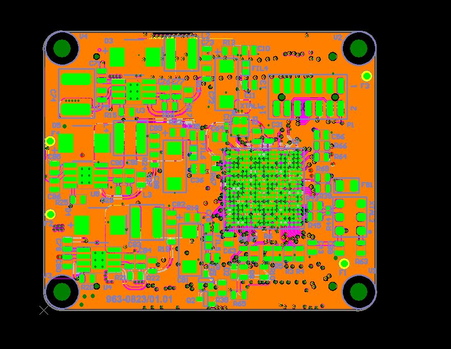
It involves issues such as reflection crosstalk, delays or emissions whenever you initiate the designing of the boards.
It is one of the most distinct designs due to the kind of attention it receives. You can use one to design a board where the main focus is on component routing and placement.
With designs of high speed, it is important to:
Such considerations are important for taking the design to a new level of functionality.
The most significant rule that you should look at is knowing the power path of the printed circuit board.
The amount of power and the location of the circuit is another significant consideration to focus on high power PCB designs.
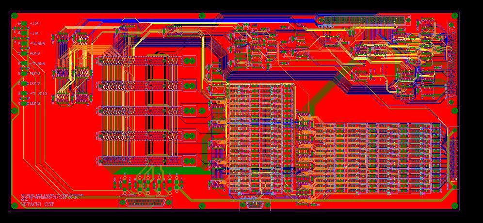
Apart from these factors, there are other factors to consider in high power PCB designs which include:
You will use this type of printed circuit board in devices that require the use of high power.
Since devices are becoming smaller and smaller by the day, PCB designs should be high power tolerant.
High-Density Interconnect printed circuit boards is one of the fastest growing technologies for the PCB designs.
HDI PCB’s contain buried and/or blind vias and microvias that are less than a diameter thick usually 0.006 micrometres.
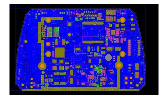
The circuitry density of this board is higher than the normal densities of the printed circuit boards.
High-Density Interconnect boards are available in six different types which include:
The benefits of using this type of printed circuit board include:
Light Emitting Diode printed circuit board is an advancement in technology for the LED lighting. It features the connection of the LED to the circuit board and a chip producing light whenever the electric current flows.
Bonding of the chips is possible through the use of ceramic bases and thermal heat sinks.
The heat it generates is very high thus cooling through traditional means is very difficult.
You will, therefore, find metal cores in LED PCB’s because of the ability to release heat.
The most common piece of metal you will find in the LED PCB is aluminium.
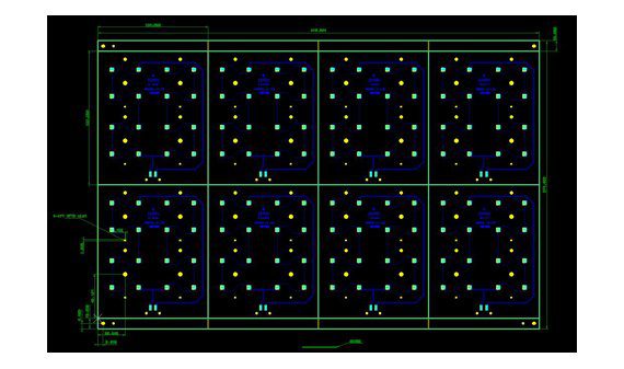
An aluminium PCB will include a thin layer of dielectric material that is able to conduct enough heat.
It is able to conduct and transfer heat from the system making it better than the traditionally printed circuit boards.
You will find the LED PCB design in different applications due to the following excellent abilities:
The applications that require the LED PCB include automotive headlights, military lighting applications, airport runway lighting, and street lighting.
Other applications are lighting in the highway tunnels, photovoltaic or solar lighting, lanterns and flashlights, signals and traffic lightings.
You may also find it in hospital lightings such as the theatre or operating rooms and growing plant lightings among others.
Radiofrequency printed circuit board designs is one of the most exciting pieces’ engineers have been working on.
You are likely to find the high-frequency boards in the upcoming technological inventions such as smartphones, robotics and sensors.
The high complexity of the design makes it an extremely difficult design to come up with.
The Industry of the printed circuit boards will consider any PCB operating above 100MHz as a radio frequency PCB.
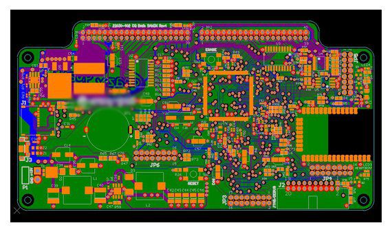
The devices that use the RF PCBs are complex and can accommodate both analog and digital signals.
There are certain devices that can accommodate different configurations of 60 layers.
The high voltage printed circuit board design is common in different applications that require very high voltages.
It is important to have enough space and suitable clearances when designing the high voltage printed circuit board.
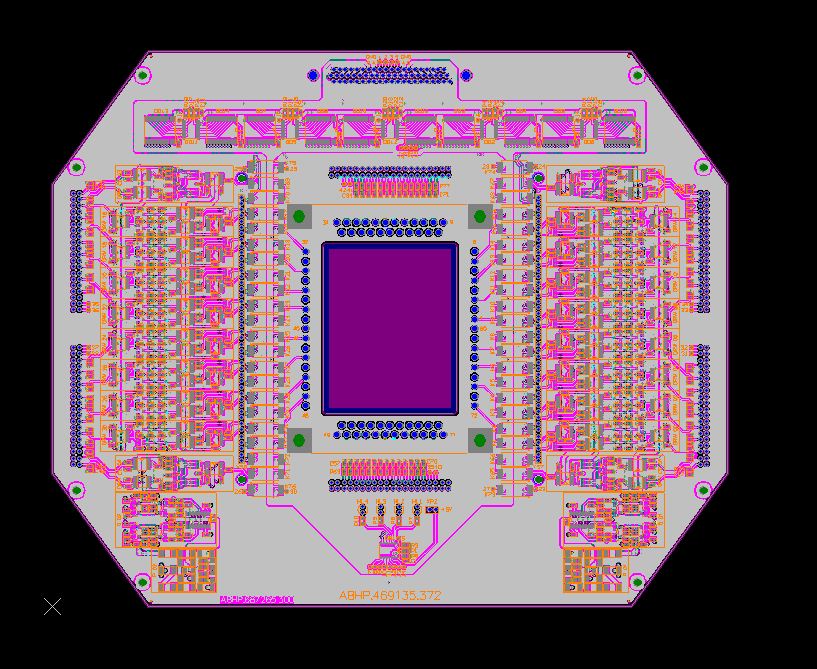
It helps in the elimination of any electrical breakdowns or electrical arcing.
When you are planning to come up with the high voltage PCB, there are certain considerations to look at.
The considerations include altitude, clearance, creepage distance, double insulation, reinforced insulation, basic insulation, supplementary insulation, and functional insulation.
The grade of insulating material, the altitude, environment, and type of PCB affect the creepage and clearance.
You are most likely to find amplifier PCB designs in devices that produce sound with low to high-frequency audio devices.
The aspects of designing a complete functional audio circuit have been a challenge since it is very complex.
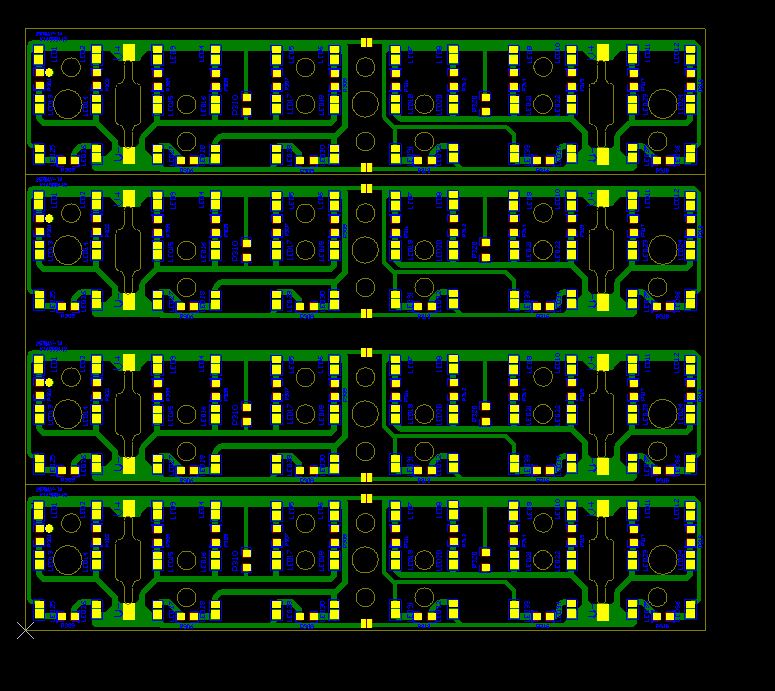
It is therefore important to have a specific layout that you will follow during the designing process.
The factors to consider when designing an amplifier PCB design are:
Metalcore printed circuit boards or MCPCB are boards that use metal as the base material to spread the heat.
The base metals come as alternatives for CEM3 or FR4 boards as it disseminates heat faster and better.
Metal core will spread the heat to other fewer heat areas such as the metallic core or heatsink backing.
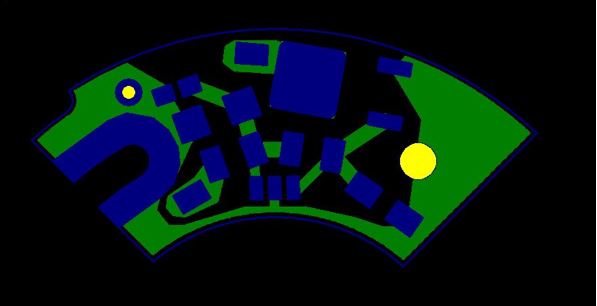
The type of metal material you can use in making the metal core printed circuit board will vary accordingly.
The most common metal materials are aluminium, copper or different mixtures of metal alloys. Again, the thickness of the metal core should range from 30 mils to 125 mils even though the thickness varies.
The advantages of using the metal core printed circuit board are as follows:
PCB layout design is the process of arranging and connecting electronic components on a printed circuit board to create a functional circuit. It starts with schematic capture, followed by strategic component placement and routing of conductive pathways. Designers consider electrical performance, manufacturability, and assembly requirements, applying design rules and DFM/DFA guidelines. The process includes simulations and prototype testing to ensure reliability. The final design is translated into manufacturing files, such as Gerber files, for PCB fabrication and assembly.
PCB designs come in various types to meet different application needs, including single-sided, double-sided, and multi-layer PCBs for varying complexity levels. Specialized types include rigid PCBs for durability, flexible and rigid-flex PCBs for space-constrained applications, high-frequency PCBs for RF and microwave use, aluminum-backed PCBs for superior heat dissipation, HDI PCBs for high-density component placement, and embedded PCBs for integrating components into the substrate. Each type is tailored to specific requirements, ensuring optimal performance, durability, and manufacturability across a wide range of electronics.
Professional terms in PCB design cover various stages and elements, from schematic creation and component placement to manufacturing and assembly techniques. Key terms include schematic diagram, Gerber files, BOM, trace, via, pad, silkscreen, solder mask, drill file, annular ring, copper pour, footprint, pick and place, SMT, THT, panelization, netlist, DFM, DRC, impedance control, thermal relief, multilayer PCB, stack-up, clearance, and blind/buried vias. Understanding these terms is crucial for efficient PCB design and manufacturing.
The cost of PCB design is calculated based on board complexity, material selection, design features, manufacturing requirements, design services, and regulatory compliance. Factors such as the number of layers, substrate material, component density, HDI features, impedance control, special finishes, prototype vs. production runs, turnaround time, testing, labor, expertise, and compliance standards all contribute to the overall cost. Understanding these elements helps in budgeting and optimizing the design process for cost-effectiveness.
PCB design is integral to numerous industries, including consumer electronics, automotive, telecommunications, medical devices, industrial automation, aerospace and defense, computing, energy and power, and instrumentation and measurement. Each industry relies on PCB technology to develop sophisticated, reliable, and efficient electronic products and systems. The versatility and critical nature of PCBs make them indispensable across a broad spectrum of applications, driving innovation and functionality in modern technology.
When choosing a PCB design service provider, consider factors such as their experience, design capabilities, quality standards, technological infrastructure, turnaround time, cost, customer support, reputation, geographical location, and scalability. Thoroughly evaluating these aspects will help you select a provider that can deliver high-quality, reliable, and cost-effective PCB design solutions tailored to your specific needs.
Selecting a PCB design software manufacturer involves evaluating functionality and features, ease of use, compatibility and integration, performance and reliability, support and community, cost and licensing, scalability, reputation and reviews, industry-specific requirements, and trial and evaluation options. Carefully considering these factors will help you choose software that enhances your design capabilities, fits your budget, and supports your long-term needs.
The choice of PCB design software depends on factors such as the complexity of your design, budget, and specific features required. Tools like Altium Designer and OrCAD are suited for high-performance and complex designs, while KiCad and Eagle are popular for their accessibility and flexibility. For quick, web-based solutions, EasyEDA and CircuitMaker offer convenient options. Each software has its strengths, making it important to evaluate them based on your design needs and workflow.
Effective PCB layout design requires adherence to design rule checks, signal integrity principles, power distribution techniques, thermal management, and manufacturability guidelines. Proper component placement, layer stack-up, and testing considerations are crucial for creating reliable and functional PCBs. Following these rules helps ensure the final PCB design is manufacturable, performs well, and meets industry standards and regulatory requirements.
The high-speed PCB design process requires a meticulous approach to handle the complexities of high-frequency signal transmission. It involves careful schematic design, precise PCB layout, signal integrity analysis, thermal and EMC considerations, and thorough testing. By following these steps, designers can create PCBs that perform reliably and efficiently in high-speed applications, ensuring optimal signal integrity and overall system performance.