


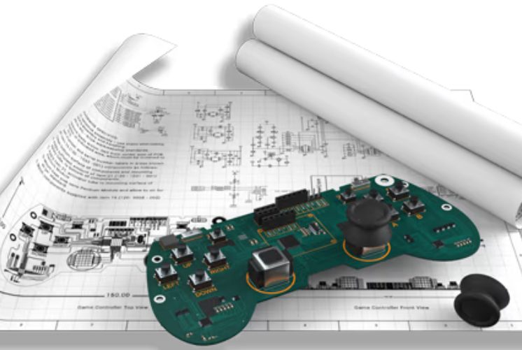
PCB Layout Planning – Packages and Routing
PCB layout planning is a critical phase in the design process, enabling engineers to save time and ensure a structured approach to package management, component placement, and routing. Proper planning ensures that the design meets electrical, spacing, and physical requirements before moving to the actual layout stage. This article explores key aspects of PCB layout planning, focusing on footprint management, routing strategies, and design for manufacturability (DFM).
Footprint Management in PCB Layout Planning
Footprints define the physical characteristics of components and their placement on the PCB. Effective footprint management during the planning phase ensures compatibility, manufacturability, and reliability. Key considerations include:
1. Package Selection
- Verify component datasheets to ensure the footprint matches the physical component specifications (e.g., pad size, spacing, and outline).
- Avoid mismatches during manufacturing and assembly by selecting the correct footprint.
2. Standardization
- Use standardized footprints to improve consistency and compatibility with automated assembly processes.
- Standardization reduces errors and streamlines production.
3. Spacing Requirements
- Manage inter-pad and inter-component spacing to prevent solder bridging and ensure effective soldering.
- Adequate spacing is critical for high-density designs.
4. Thermal Considerations
- Incorporate thermal vias or pads in footprints for heat-generating components.
- Ensure proper thermal management to avoid overheating and reliability issues.
How to Prepare Footprints for Layout
| Category | Guide | Purpose |
|---|---|---|
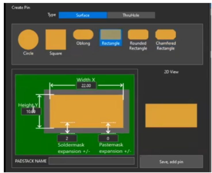
| Verify Component Datasheet | Use manufacturer datasheets to confirm pad size, spacing, and outline. | Ensure compatibility with physical components. |
| Follow IPC Standards | Design footprints compliant with IPC standards for pad size and solder mask. | Adhere to industry standards for reliable assembly. |
| Optimize Pad Size | Define pad size based on component type to prevent solder bridging. | Enhance solderability and assembly reliability. |
| Include Orientation Markers | Add silkscreen markings for pin 1, polarity, and component orientation. | Prevent assembly and alignment errors. |
| Design for Manufacturability (DFM) | Ensure adequate clearance between pads, drill holes, and PCB edges. | Improve manufacturability and reduce production issues. |
| Minimize Assembly Risk | Use symmetrical pad layouts to avoid tombstoning and ensure consistent fillets. | Reduce soldering defects and improve assembly quality. |
Planning for Specialized Components
1. Surface Mount Devices (SMDs)
- Focus on precise pad definition, keep-outs, and solder mask bridges.
- Ensure adequate spacing for stencil printing and reflow soldering.
2. Through-Hole Components
- Define drill hole dimensions, annular rings, and pad stacks for robust mechanical connections.
- Ensure proper alignment with the PCB layout.
3. High Pin Count Components (e.g., BGAs)
- Plan for proper spacing, alignment, and thermal management.
- Use via-in-pad or microvias for high-density designs.
PCB Layout Planning Considerations
1. Functional Grouping
- Place related components in close proximity to minimize trace lengths and improve signal integrity.
- Group power, analog, and digital components separately to reduce noise.
2. Signal Prioritization
- Prioritize routing for high-speed signals, sensitive analog lines, and power distribution.
- Use controlled impedance routing for critical signals.
3. Mechanical Constraints
- Align components with housings, connectors, and mounting holes.
- Maintain adequate edge clearance for traces and components.
4. Thermal Design
- Strategically place heat-generating and heat-sensitive components.
- Optimize airflow and cooling by incorporating thermal vias and heatsinks.
PCB Layout Planning Checklist
| Preparation Phase | Key Details |
|---|---|
| BOM Verification | – Verify Manufacturer Part Number (MPN) and Vendor Part Number (VPN). |
| – Check component availability to avoid obsolete parts or long lead times. | |
| – Mark “Do Not Install” (DNI) components clearly. | |
| Stack-up Design | – Select materials (e.g., FR4, Rogers) based on frequency and environmental needs. |
| – Define layers for signal, power, and ground planes. | |
| – Establish controlled impedance (e.g., 50Ω single-ended, 100Ω differential). | |
| – Select copper thickness (½ oz, 1 oz, or 2 oz). | |
| Design Rule Definition | – Set electrical rules for impedance, resistance, and high-frequency design. |
| – Define physical rules for trace width, via size, and clearance. | |
| – Specify spacing rules for traces, vias, and copper-to-edge distance. | |
| Schematic and Netlist Preparation | – Create component symbols with reference identifiers linked to footprints. |
| – Ensure netlists define connections and critical signal paths clearly. | |
| – Label impedance-controlled lines and power nets for easy identification. | |
| Board Outline Definition | – Define board size and shape manually or by importing CAD data. |
| – Align outlines with enclosure design and mechanical constraints. | |
| – Allow adequate edge clearance for traces and components. | |
| DFM Considerations | – Maintain minimum trace widths and spacing per manufacturing guidelines. |
| – Avoid complex assembly features like via-in-pad unless necessary. | |
| – Ensure silkscreen and solder mask are clear and legible. |
Effective PCB layout planning is essential for creating high-performance, manufacturable designs. By focusing on footprint management, routing strategies, and DFM considerations, engineers can streamline the design process and ensure reliability. Leveraging advanced tools like Cadence Allegro PCB Designer can further enhance efficiency and precision in layout planning. Whether working on simple or complex designs, a structured approach to PCB layout planning ensures success in meeting electrical, mechanical, and thermal requirements.