


PCB Edge Plating: Enhancing Connectivity and Durability
PCB edge plating is a specialized process that involves applying a metal coating to the exposed copper connections at the edge of a printed circuit board (PCB). This technique, also known as side plating, battlement, or metallized edge plating, enhances electrical connectivity, structural rigidity, and electromagnetic interference (EMI) shielding. This article provides an in-depth look at the PCB edge plating process, its benefits, materials, and application methods.
PCB Edge Plating Process Overview
The edge plating process involves several steps to ensure a durable and conductive metal coating on the PCB edges. Below is a step-by-step breakdown of the process:
| Process Steps | Description |
|---|---|
| Design | Designers specify which board edges require plating for connectors or components. |
| Panelization | Multiple PCBs are fabricated on a larger panel for efficiency. Edge plating is applied to the entire panel before separation. |
| Drilling for Edge Contacts | Via holes are drilled along the edge to provide access points for electroplating. |
| Surface Preparation | PCB edges are cleaned, degreased, and roughened to ensure good plating adhesion. |
| Electroless Plating | A thin layer of electroless copper is applied as a foundation for electroplating. |
| Plating | Additional copper is plated to achieve the desired conductivity and durability. |
| Etching | Excess copper is chemically etched to define and isolate the desired traces. |
| Tin or Other Finishes | A final coating (e.g., tin, gold) is applied to improve solderability and corrosion resistance. |
| Routing and Separation | The PCBs are separated from the panel, leaving the plated edges intact. |
| Quality Control | Checks ensure the plating meets thickness and continuity specifications. |
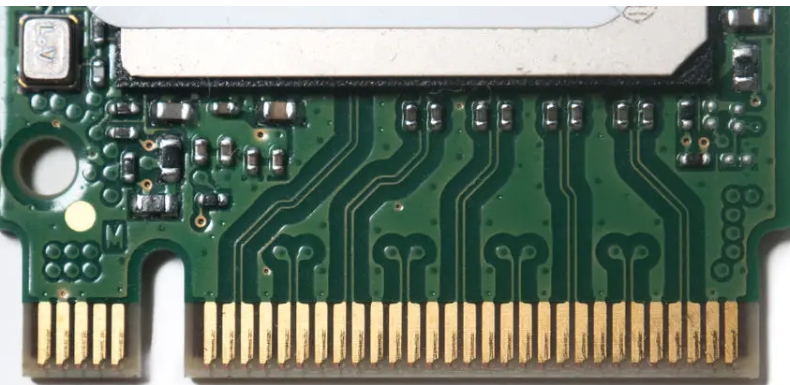
What is PCB Edge Plating?
PCB edge plating involves coating the sidewalls of the PCB substrate with conductive material, typically copper, which extends from the top to the bottom surface and along one or more perimeter edges. This process is also referred to as:
- Metallized edge plating
- Boundary plating
- Side plating
- Battlement
Edge plating can be applied to a single edge or multiple edges of the PCB, depending on the design requirements.
Benefits of PCB Edge Plating
- EMI Shielding:
- Edge plating provides a continuous conductive path along the PCB edge, reducing electromagnetic interference (EMI) and improving signal integrity.
- Chassis Grounding:
- It enhances chassis grounding, ensuring a reliable electrical connection between the PCB and the enclosure.
- Structural Rigidity:
- Edge plating adds strength to the PCB, making it more resistant to bending and warping, which is especially important for larger or rigid boards.
- Reliable Electrical Connections:
- It ensures consistent and reliable electrical connections at the edge of the PCB, which is critical for edge-mounted connectors and components.
Materials Used in PCB Edge Plating
The most common materials used for edge plating include:
- Copper: Provides excellent conductivity and forms the base layer for plating.
- Gold: Offers superior corrosion resistance and solderability.
- Silver: Used for high-conductivity applications.
- Tin: Improves solderability and is cost-effective.
- Nickel: Adds durability and acts as a barrier layer.
Types of PCB Edge Plating
- Regular Plane Edge Plating:
- Standard edge plating applied to the perimeter of the PCB.
- Edge Plating:
- Custom plating applied to specific edges for connectors or components.
- Ripple Edge Plating:
- A specialized plating technique used for high-frequency or high-power applications.
Application Methods for PCB Edge Plating
- Isolated Copper Structure:
- Edge plating is applied as a separate copper structure, isolated from other copper pours on the PCB. This method is commonly used for chassis ground connections.
- Polygonal Overlay:
- A polygonal overlay encircles the PCB edge, extending back to the opposing surface layer. This technique is used for system ground connections and requires top-layer clearance.
Applications of PCB Edge Plating
- Edge-Mounted Connectors: Ensures reliable electrical connections for connectors placed at the edge of the PCB.
- High-Frequency Circuits: Provides EMI shielding and improved signal integrity.
- Industrial and Automotive Electronics: Enhances durability and grounding in harsh environments.
- Large or Rigid PCBs: Adds structural strength to prevent bending or warping.
PCB edge plating is a critical process that enhances the electrical, mechanical, and thermal performance of printed circuit boards. By providing EMI shielding, improving chassis grounding, and adding structural rigidity, edge plating ensures reliable and durable PCB designs. Whether used for edge-mounted connectors, high-frequency circuits, or industrial applications, edge plating is an essential technique for modern PCB manufacturing.