PCB Design for the 6-Layer Board Stackup
There are some things in life that seem to set the standard for whatever area that you are currently involved in. Some will always compare baseball players to Jackie Robinson, while others will say that nobody could carry a tune the way that Elvis did. For me, I tend to equate the standard printed circuit board as being a 6-layer design.
Back when I first started laying out circuit boards, the 6-layer board seemed to be the workhorse of PCB design world. Although we did design many other boards that had different multiple layer configurations, those 6-layer jobs is what I tend to remember the most. There still is a great need for the 6-layer board stackup as they serve many different needs, and as such, there are different ways that they can be configured. Here’s a little more information on those board configurations and how you can best use them.
The Importance of a 6-Layer Board Stackup in PCB Design
Multilayer printed circuit boards have been a staple of the design world now for decades. As electronic components have shrunk and thereby allowing more circuitry to be designed onto one board, their capabilities have increased the need for new PCB design and manufacturing technologies to support them. At one time the 6-layer board stackup was merely a way to get more traces onto the board than what either a 2 or 4 layer board allowed for. Now it is more important than ever to create the correct configuration of layers in a 6-layer stackup to maximise the performance of the circuitry.
A PCB layer stackup that is not configured correctly will be susceptible to electromagnetic interference (EMI) due to poor signal performance. On the other hand, a well designed 6-layer stackup can prevent problems caused by impedance and crosstalk and improve the performance and reliability of the circuit board. A good layer stackup configuration will also help to protect the board from external noise sources. Here are some examples of 6-layer stackup configurations.

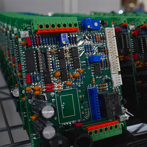
An example of a printed circuit board with a 6-layer board stackup
What is the Best 6-Layer Stackup Configuration?
The stackup configuration that you choose for your 6-layer board will depend a lot on what you need to accomplish with your design. If you have a lot of signals that need to be routed, you will want 4 signal layers to route on. On the other hand, if control over the signal integrity of high speed circuits is the priority, you will want to choose the option that offers the best protection. Here are some of the different configurations that are in use in 6-layer boards.
The first layer stackup option is the original stackup configuration that I first started working with many years ago:
- Top Signal
- Inner Signal
- Ground Plane
- Power Plane
- Inner Signal
- Bottom Signal
This is probably the worst configuration that you can use as there isn’t any shielding for the signal layers, and two of the signal layers are not adjacent to a plane. As signal integrity and performance requirements became more important, this configuration was generally abandoned. However, by replacing the top and bottom signal layers with a ground plane, you once again have a good 6-layer stackup. The disadvantage is that it leaves you with only two internal layers for signal routing.
The most commonly used 6 layer configuration in PCB design is to put the inner signal routing layers in the middle of the stackup:
- Top Signal
- Ground Plane
- Inner Signal
- Inner Signal
- Power Plane
- Bottom Signal
The configuration of the planes provide better shielding for the inner signal routing layers, which are normally used for higher frequency signals. This stackup can be even better enhanced by increasing the distance between the two inner signal layers with a thicker dielectric material. The drawback to this configuration though is that the separation of the power and ground planes reduces their planner capacitance. This will require adding more decoupling into the design.
The 6-layer stackup that is configured to give a PCB the best signal integrity and performance is one that isn’t so common. Here the signal layers are reduced to 3 in order to add an additional ground layer:
- Top Signal
- Ground Plane
- Inner Signal
- Power Plane
- Ground Plane
- Bottom Signal
This stackup places each signal layer immediately adjacent to a ground plane for the best return path characteristics. Additionally, by having the power and ground plane next to each other creates planner capacitance. The disadvantage again though is that you do lose one signal layer for routing.

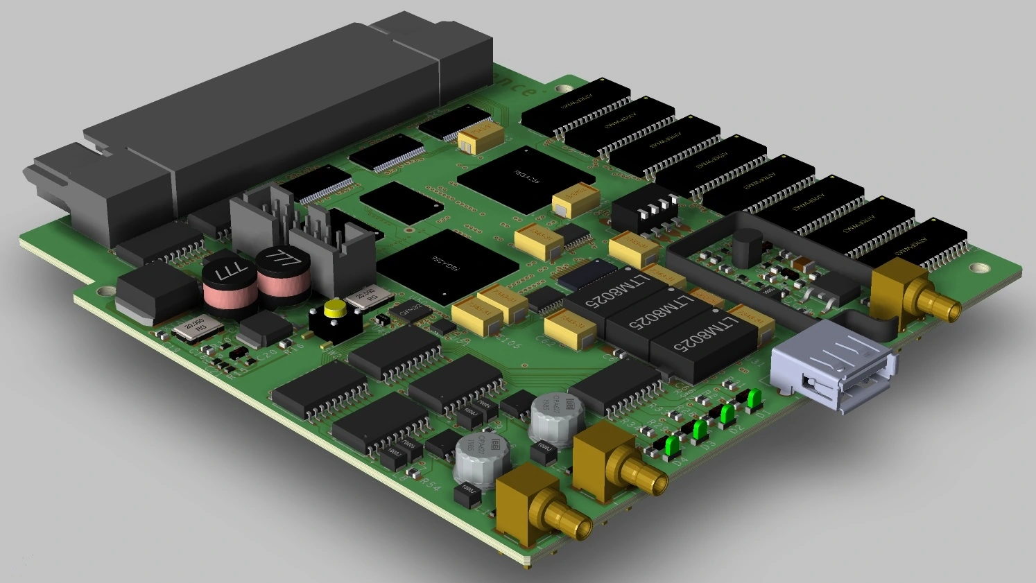
Using the right PCB design tools will better help you to configure your 6-layer board stackup
Put Your PCB Design Tools to Work
How you create your board layer stackup will have a huge impact on the success of your 6-layer PCB design. Fortunately today’s PCB design tools will give you the ability to add and delete layers from your design so that you can choose whichever layer configuration that best suits your needs. The important part is to choose a PCB design system that gives you the maximum amount of flexibility and power so that you can easily create the type of 6-layer stackup for your design.
An example of a PCB design system that has all the to do what we’ve talked about here is from Cadence. OrCAD PCB Designer has the functionality to configure a 6-layer board, or any other type of PCB layer stackup to fit your exact needs. Additionally, OrCAD gives you many powerful features and functionality to place, route, and setup design rules and constraints so that your design is built the way you intended it to be.
If you’re looking to learn more about how KKPCB has the solution for you, talk to us and our team of experts.


