


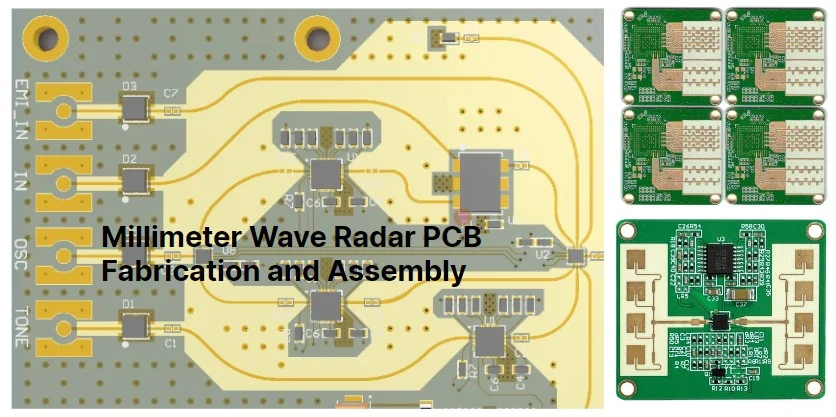
PCB Design and Processing for Millimeter-Wave Circuits (Part 2)
PCB Processing
The precise dimensions required for millimeter-wave circuits demand well-controlled PCB processing techniques to produce circuits with consistently excellent performance. Variations in copper plating thickness and final surface treatment on the conductor surface can impact the performance of millimeter-wave circuits. To ensure the successful fabrication of high-performance millimeter-wave circuits, both of these processes must be carefully controlled.
For laminates, the original copper thickness variation is typically controlled within a ±10% tolerance range. For circuits with plated through-holes (PTH) for interconnections, the final circuit’s copper plating is usually thicker to support the PTH process. The normal variations in copper plating thickness depend on the circuit design and processing techniques. During circuit fabrication, multiple circuits are typically produced on a large panel. In general, the plated copper tends to be thinner in the middle and thicker at the edges. This variation in copper thickness can lead to performance fluctuations at millimeter-wave frequencies. In high-volume production of millimeter-wave circuits, variations in copper thickness can cause differences in insertion loss and phase response between circuits. GCPW circuits and most circuits with coupled circuit characteristics are particularly susceptible to variations in copper thickness.
A few years ago, we conducted a study using a 10-mil hydrocarbon-based material to evaluate the performance variations of circuits with different copper thicknesses. To minimize the impact of dielectric variations, all dielectric materials were taken from the same batch. A 24″ × 18″ (610 × 457 mm) circuit material panel was cut in half, with one half processed using thin copper plating and the other using thick copper plating. Each half-panel was fabricated with identical circuits, including microstrip circuits, tightly coupled, and loosely coupled GCPW transmission line circuits. The total copper thickness for the circuits with thin copper plating was 1 mil, while for the thick copper circuits, it was 3 mil. Of course, a 3-mil copper thickness variation is unlikely to occur in large-scale production; this study was conducted solely to highlight the impact of thickness variation.
Among these different circuits, the single-ended microstrip transmission line circuits showed minimal differences in performance between the thin and thick copper circuits. The insertion loss and effective Dk of the thick copper circuits were slightly lower than those of the thin copper circuits. The thicker copper conductors created more fringing fields in the air, resulting in a slight decrease in the effective Dk and a slight reduction in insertion loss. However, at millimeter-wave frequencies, microstrip transmission lines with thicker copper can introduce more interference issues due to increased surface wave propagation on the thicker conductors at such short wavelengths.
In contrast, significant differences were observed in tightly coupled single-ended GCPW transmission line circuits due to copper thickness variations (see Figure 5). Each circuit was labeled based on its signal conductor width (w) and the spacing (s) between the conductor and adjacent ground layers. For example, a tightly coupled circuit with a signal conductor width of 18 mil and a spacing of 6 mil was labeled w18s6, while a loosely coupled circuit had dimensions of w21s10.
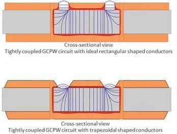
Figure 5: The cross-sectional view of GCPW circuit dimensions, where the left image represents a circuit with thin copper plating, and the right image shows a circuit with thick copper plating.
Compared to GCPW circuits with thinner copper conductors, circuits with thicker copper conductors generate more electric fields in the air. Additionally, thicker copper conductors are more likely to create a trapezoidal shape rather than a rectangular one. The shape of the conductor influences the electric field characteristics, which in turn affects the millimeter-wave performance.
Figure 6 shows the comparison of insertion loss between tightly coupled and loosely coupled GCPW transmission line circuits with thin and thick copper conductors, based on real measurements. The circuits ensured that the return loss was greater than 15 dB across the frequency range of 66 GHz to 68 GHz, eliminating the impact of return loss. It can be seen that the thick copper conductor GCPW circuit with a conductor width of 21 mil and a spacing of 12 mil (w21s12) has the lowest insertion loss. This is because the thicker copper conductors generate more electric field in the air; air has minimal loss, and the wider conductor reduces conductor loss, leading to the overall lowest insertion loss. In contrast, the thin copper conductor GCPW circuit with a conductor width of 18 mil and a spacing of 6 mil (w18s6) has the highest insertion loss. This is because it has the lowest proportion of electric field in the air, and the narrower signal conductor increases conductor loss, resulting in the highest overall insertion loss.
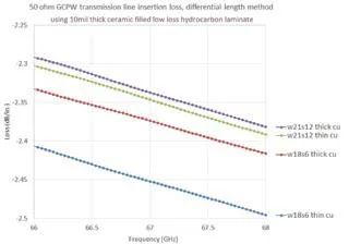
Figure 6: Comparison of insertion loss for loosely coupled (w21s12) and tightly coupled (w18s6) GCPW circuits with thin and thick copper conductors.
The phase angle measurements at different frequencies can also be used to evaluate the effective Dk of the circuit based on its phase response. Transmission lines of different lengths have different phase delays. At a specific frequency, the relationship between the length difference and the phase angle delay difference is fixed. The differential phase-length method can be used to determine the effective Dk value of each circuit. In this testing method, two identical circuits are measured, ensuring that the phase angle difference reflects the material properties. These two circuits are placed side by side on the same circuit material board to ensure identical dielectric and copper foil characteristics. This allows the phase difference to reflect the material’s inherent properties, and the effective Dk value can be calculated using a formula that relates phase angle difference and physical length difference.
Figure 7 shows that the GCPW circuit with the lowest effective Dk value is the thick copper conductor circuit with a conductor width of 18 mil and a spacing of 6 mil (w18s6). Since this is a tightly coupled circuit, the electric field increases in the coupling area (in the air). The thicker copper conductor results in higher coupling sidewalls, causing more electric field to exist in the air, which further reduces the effective Dk value. The GCPW circuit with the highest effective Dk value is the thin copper conductor circuit with a conductor width of 21 mil and a spacing of 12 mil (w21s12), as it has less electric field distribution in the air.
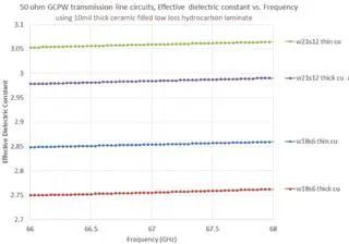
Figure 7: Comparison of the effective Dk values for tightly coupled (w18s6) and loosely coupled (w21s12) GCPW circuits with thin and thick copper conductors.
Many millimeter-wave circuits (such as 5G small cells and radar systems) rely on maintaining consistent and accurate phase responses, so it is crucial to keep the phase angle deviation within an acceptable range across the application frequency range. For example, as mentioned earlier, for a 77 GHz radar, the total phase delay of the circuit can be several thousand degrees, making a phase deviation range of 50° or (±25°) acceptable. Depending on the design, some radar systems may allow larger phase deviations, while others may require phase deviations of no more than ±10°. PCB designers and manufacturing engineers should be aware of the impact of circuit material characteristics and PCB fabrication processes on the circuit’s phase response, particularly for circuits operating at millimeter-wave frequencies with short wavelengths. For example, the Dk value variation shown in Figure 7 of 0.1 translates to a phase angle change of about 60° in the 67 GHz frequency band. This phase angle change is primarily caused by copper thickness variation, but other factors, including dielectric material thickness variation, Dk variation, and surface treatment, also affect phase angle changes. In GCPW circuits, the final copper thickness variation significantly affects the coupling characteristics, thereby impacting the phase. However, microstrip circuits are less affected by copper thickness variation, making them more suitable for signal transmission at millimeter-wave frequencies.
It is also necessary to evaluate how the final surface treatment of the circuit affects insertion loss. At millimeter-wave frequencies, surface treatment plays an important role in the circuit’s phase angle response. The impact of surface treatment on performance generally depends on the type of circuit (e.g., single-ended or coupled circuits) and the influence of skin depth at different operating frequencies.
Figure 8 shows how surface treatment affects the insertion loss of microstrip transmission line circuits. The test circuit used rolled copper to minimize the impact of copper foil roughness, and different thicknesses of electroless nickel immersion gold (ENIG) surface treatments were applied to compare changes in the circuit’s loss. The ENIG process typically results in a certain thickness variation in the nickel layer, which can affect the insertion loss and phase response of circuits at millimeter-wave frequencies.
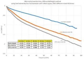
Figure 8: Comparison of insertion loss differences in microstrip transmission line circuits with different nickel plating thicknesses, using bare copper circuits as the reference.
The results in Figure 8 also demonstrate the edge effects of final surface treatments. In microstrip circuits, the RF current and electric field are primarily concentrated on the left and right edges of the signal conductor. When the conductor edges are coated with metals that have poorer conductivity than copper, conductor losses will increase, thereby increasing the total insertion loss of the circuit. However, in GCPW circuits, which include four conductor edges, the impact of the surface treatment layer is more significant than in microstrip circuits, which only have two conductor edges. Figure 9 shows test results for tightly coupled GCPW circuits, revealing that the impact of the surface treatment layer on GCPW circuits is more significant compared to microstrip circuits shown in Figure 8.
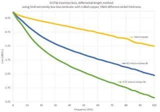
Figure 9: Comparison of insertion loss differences in GCPW transmission line circuits with different nickel plating thicknesses, using bare copper circuits as the reference.
The reference circuits in Figures 8 and 9 are bare copper circuits without surface treatment, compared to circuits with surface treatment layers. Circuit designers typically use specific material parameters (such as Dk, Df) for design and simulation, but these simulations do not account for the influence of surface treatment layers. These layers’ effects are difficult to model and simulate in software, but they become more pronounced as the frequency increases, affecting insertion loss and phase response in both microstrip and GCPW circuits.
Figure 10 illustrates how PCB surface treatment affects the effective Dk value of tightly coupled GCPW circuits in the 70-80 GHz range, and the resulting phase response changes. The difference in effective Dk values between circuits with thin and thick nickel plating is around 0.02. Compared to microstrip circuits, the difference in effective Dk values for tightly coupled GCPW circuits caused by plating thickness variations is more pronounced, indicating that plating thickness changes lead to greater phase response deviations in GCPW circuits. A 0.02 difference in effective Dk corresponds to a phase angle shift of about 60° in the 70-80 GHz range. This significant phase angle deviation may be problematic for millimeter-wave applications that require phase consistency, such as radar systems and 5G NG wireless networks.
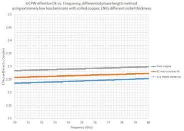
Figure 10: Comparison of the impact of different nickel plating thicknesses on the effective Dk value of GCPW transmission line circuits, using bare copper circuits as the reference.
To minimize the impact of surface treatment layers on insertion loss and Dk at higher frequencies, most millimeter-wave circuits avoid using ENIG, as the nickel plating thickness variation in ENIG can lead to significant and widespread phase angle changes. As a low-loss alternative, processes like Immersion Tin (ImSn) and Immersion Silver (ImAg) are more commonly used for millimeter-wave PCBs. In addition, some organic solderable preservative (OSP) coatings, which offer low loss and long shelf life, are also used for millimeter-wave circuits. Although ImSn slightly increases insertion loss and causes phase response variations, its thin plating results in smaller thickness variations, leading to less impact on millimeter-wave circuit performance compared to ENIG.
Figure 11 shows the impact of Immersion Tin thickness on insertion loss from low frequencies to 70 GHz. The test data extends up to 110 GHz, as circuits above 70 GHz experience poorer return loss and some fluctuation in insertion loss, so results above 70 GHz are not displayed, but the trend remains similar. At 70 GHz, the insertion loss difference between microstrip circuits with thin and thick ImSn plating is approximately 0.12 dB/in, which is much smaller than the insertion loss variation caused by ENIG thickness differences at the same frequency (shown in Figure 8). Similarly, the phase angle difference caused by changes in ImSn plating thickness is slightly less than 3° at 70 GHz.
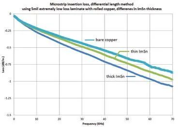
Figure 11: Comparison of the effect of Immersion Tin plating thickness on microstrip circuit loss, using 5 mil low-loss rolled copper circuit material.
Conductor Shape
Due to the small wavelength of millimeter-wave circuits, the etching of circuit conductors must be more precise and repeatable. Whether for coupled circuits (such as GCPW) or microstrip circuits, the conductor should be as close to an ideal rectangular shape as possible, minimizing trapezoidal conductor shapes. The conductor shape becomes more critical at higher frequencies; for example, at 77 GHz, a trapezoidal conductor shape has a more significant impact on circuit performance than at 24 GHz. Additionally, the effect of trapezoidal conductors is more pronounced on narrower conductors than on wider ones. Typically, circuits designed for 77 GHz use thinner laminate boards (e.g., 4 mil or 5 mil thick) to avoid unnecessary higher-order mode propagation. As a result, the signal conductors in these circuits are narrower, making the trapezoidal shape more noticeable and affecting performance. In contrast, at lower frequencies (such as 24 GHz), thicker laminate boards are usually used, leading to wider signal conductors and a smaller trapezoidal effect, which has less impact on performance.
Changes in trapezoidal conductor shape can cause performance variations in GCPW and microstrip circuits due to changes in edge field distribution. Because electromagnetic waves propagate in the air with a lower Dk characteristic, this can alter the effective Dk value of the circuit compared to the ideal rectangular conductor design. For conductors with noticeable trapezoidal shapes, the electromagnetic field in the air is less, and compared to the ideal rectangular conductor, the lower Dk of the air increases the overall effective Dk value of the circuit. This effect can be characterized by phase angle response changes, especially in millimeter-wave circuits, which are more phase-sensitive. Furthermore, this effect is more significant in coupled circuits (such as GCPW) than in microstrip circuits (Figure 12).
Figure 12: Cross-sectional views showing how differences in GCPW conductor shape affect the circuit’s electric field, with the top image showing a rectangular conductor and the bottom image showing a trapezoidal conductor.
Due to thick copper plating or insufficient copper removal during the rapid etching process, the conductor may not form an ideal rectangular shape and may end up being trapezoidal. In high-volume PCB production, rapid etching processes often leave copper burrs on the left and right edges of the conductor, which can cause phase distortion in microstrip and GCPW circuits. Using thinner copper foil laminates or copper plating and well-controlled (though typically slower) etching processes are more favorable for producing rectangular conductors, ensuring better phase consistency in high-volume production.
The use of solder mask ink (green ink) in PCB production can increase insertion loss and phase deviations in high-frequency circuits, especially in millimeter-wave circuits, so it must be carefully removed. For example, in high-frequency microstrip and GCPW circuit production, liquid photoimageable solder mask (LPI) layers are typically used. If the solder mask on the microstrip conductor is not removed, the electric field that should be in the air may instead reside in the solder mask, causing changes in insertion loss and phase angle. For coupled circuits like GCPW, the impact of solder mask on insertion loss and phase response is more significant.
Depending on signal frequency and wavelength, minimizing the use of solder mask is preferred, but when necessary, solder dams can be used to reduce the impact on millimeter-wave circuit performance. Solder mask typically does not affect circuit performance beyond one-tenth of the wavelength at the operating frequency. For example, for a 77 GHz circuit, one-tenth of the wavelength is approximately 10 mil, and a solder mask larger than this will not affect circuit performance. Conversely, at 24 GHz, one-tenth of the wavelength is around 33 mil, and a solder mask of this size will not cause resonance or affect circuit propagation characteristics.
The roughness of the copper foil at the substrate-copper interface also affects phase response at millimeter-wave frequencies. The roughness can vary from one copper foil batch to another, or even within the same foil, causing phase shifts in millimeter-wave circuits. For instance, the average copper foil surface roughness of a certain ED copper is 2 µm RMS, but the variation can range from 1.7 to 2.3 µm, leading to noticeable phase response and insertion loss variations at millimeter-wave frequencies.
In conclusion, due to the small wavelength, the performance of millimeter-wave PCBs relies heavily on precise circuit feature fabrication and component accuracy. Variations in processing tolerances, phase changes, and other factors are crucial for applications ranging from autonomous vehicle radar sensors to 5G wireless networks. Whether for radar target detection (collision avoidance) or phase-modulated communication, phase accuracy is critical for these applications.