


PCB Design and Fabrication for Millimeter-Wave Circuits (Part 1)
Key Points of Millimeter-Wave Applications—Phase Accuracy Affected by Multiple Variables
From anti-collision radar systems used in autonomous vehicles to the fifth-generation (5G) high data rate New Radio (NR) networks, the application of millimeter-wave (mmWave) circuits is growing rapidly. Many applications are pushing the operating frequency bands to higher frequencies (such as >24GHz). However, for circuits with shorter wavelengths, even small variations in design and fabrication can cause significant performance differences in electronic products. Understanding the differences between mmWave frequencies and lower frequency PCB circuits can help avoid performance anomalies and discrepancies.
Overview of PCB RF Technology
Compared to low-frequency circuits, high-frequency RF/microwave circuits are more susceptible to the influence of circuit materials and manufacturing processes. While circuit functions such as power lines and digital controls can be implemented using low-cost FR-4 materials, RF, microwave, and mmWave circuits require better-performing materials to minimize signal loss and distortion. Many multi-layer mixed-signal PCBs, which have various electrical functions, are typically made from a combination of different circuit materials. The most suitable material should be selected for each layer of the circuit based on its function.
High-frequency PCBs generally rely on three common transmission line technologies: microstrip circuits, stripline circuits, or ground-coupled coplanar waveguide (GCPW) circuits (see Figure 1). The figure shows the electric field (E) and current density for each circuit type based on single-ended transmission lines. It can be seen that each circuit type has a distinct structure, with the electric field representing the coupling area between the conductor and the ground plane. For differential circuits, there is also coupling between the two conductors. For example, in a differential microstrip circuit, the electric field will couple between the signal conductors on the top layer and between the top layer and the ground plane. Especially at higher frequencies, high-frequency circuits using these transmission lines are highly sensitive to circuit material parameters and PCB processing.
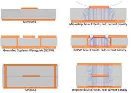
Figure 1: Cross-sectional views of three common high-frequency circuit types: microstrip, ground-coupled coplanar waveguide (GCPW), and stripline circuits (left), and their respective electric fields (E) and current density (right).
The description of the three circuit types in Figure 1 is simplified, and this description will change with frequency. At higher frequencies, the current density in the cross-section will become shallower due to the skin effect, and the electric field will be more concentrated. The electromagnetic waves (EM) (electric and magnetic fields) for each circuit propagate in a direction perpendicular to the two-dimensional circuit diagram, out of the page.
The performance of these three high-frequency transmission lines is determined by the dielectric material. In stripline circuits, the conductor is surrounded by dielectric material. In microstrip and GCPW circuits, the electric field extends outside the dielectric material, including the surrounding air, forming the circuit’s entire electromagnetic environment. Therefore, the dielectric constant (Dk) of these two circuits reflects the Dk of the substrate material and the Dk of air (which is approximately 1), resulting in what is known as the “effective Dk.”
The GCPW in Figure 1 is a tightly coupled GCPW circuit, with a small gap between the signal conductors on the top coplanar layer and the ground plane. A larger gap indicates a loosely coupled GCPW circuit. Tightly coupled GCPW circuits have a larger proportion of the electric field in the air, while loosely coupled GCPW circuits have more of the electric field within the dielectric substrate material (which has a higher Dk than air). Therefore, the effective Dk for tightly coupled GCPW is lower than that for loosely coupled GCPW.
Signal power in circuits typically decreases with frequency, so it is essential to minimize signal loss in high-frequency circuits. Maintaining impedance matching is key to reducing losses in interconnects within high-frequency circuits or systems, such as the transmission line between a signal generator and a load, as shown in Figure 2. Even if the generator and load are impedance-matched, passive components (such as high-frequency transmission lines) will still experience insertion loss due to dielectric and conductor losses. However, when impedance mismatch occurs (see Figure 2b), signal reflection at the transmission connection increases return loss, further raising the total transmission line loss from 3dB (in the matched case) to 6dB. Minimizing insertion and return losses is crucial to ensure signal power at the receiving end. These losses can be measured using a vector network analyzer (VNA), where insertion loss is measured using the S21 scattering parameter, and return loss is measured using the S11 scattering parameter.
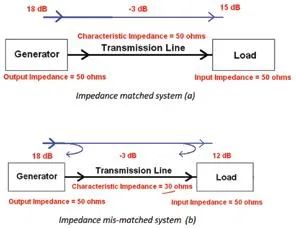
Figure 2: Losses in a transmission line with impedance matching (a) and a transmission line with impedance mismatch (b).
Insertion loss in high-frequency circuits is the sum of several different losses, including conductor loss (from the conductor), dielectric loss (from the substrate material), radiation loss (from energy radiation), and leakage loss (from energy leakage between copper layers). Reducing any of these losses will reduce the overall insertion loss in high-frequency circuits.
Leakage loss is generally a concern in materials with relatively low volume resistivity, such as semiconductor materials. However, leakage loss can usually be neglected in high-frequency PCB materials with higher volume resistivity. On the other hand, leakage loss may be significant in high-power circuits, but it is not a major concern in mmWave circuits with small signal power. Radiation loss is a notable loss at millimeter-wave frequencies and should be considered when simulating total insertion loss in the circuit. For now, we will focus on conductor and dielectric losses in the discussion of insertion loss.
Breaking down the insertion loss for circuits with different substrate thicknesses, for circuits with thin substrate materials, conductor loss dominates because the signal is closer to the ground plane, concentrating the electric field under the conductor. For thicker substrate circuits, the signal is farther from the ground plane, so conductor loss is a smaller portion of the total insertion loss, with dielectric loss dominating. Figure 3 shows how conductor loss (versus dielectric loss) in microstrip circuits changes with the thickness of the substrate.
Figure 3: For thicker circuits, conductor loss is a smaller part of the total insertion loss in microstrip circuits.
Figure 3 shows the total insertion loss for a 50Ω microstrip transmission line circuit. All circuits use the same 50Ω design and copper-clad substrate, with only thickness varying. The measured circuit loss (purple) aligns closely with the modeled total insertion loss (green), further confirming the accuracy of the model. The breakdown of dielectric and conductor losses at various substrate thicknesses is also displayed.
Figure 3 also shows how conductor loss varies with substrate thickness for circuits using the same dielectric material. The roughness of the copper foil at the interface between the dielectric substrate and copper foil also affects conductor loss. A rougher copper foil surface increases conductor loss compared to a smoother surface. Copper foil roughness also influences the Dk value of the circuit, as rougher copper foil increases the propagation path of electromagnetic waves, forming a slow-wave effect, which increases the effective Dk value and introduces phase delay.
High-frequency designs typically require the use of thinner substrate materials, and low insertion loss is a critical factor at high frequencies. In this case, the type of copper foil also becomes a significant consideration. The smoother the copper foil, the lower the insertion loss. For example, comparing conductor loss at different thicknesses in Figure 3, it can be seen that conductor loss dominates in thinner circuits. Therefore, smoother copper foils can be selected to reduce conductor losses. Nonetheless, reducing insertion loss can also be achieved by controlling dielectric loss. Therefore, choosing materials with low loss factors (Df) can further reduce the total insertion loss of the circuit. For example, in Figure 3, the Df of the material is 0.0037, but if a material with a Df of 0.0010 is used, dielectric loss (and insertion loss) will further decrease.
Phase Accuracy
In many high-frequency circuits, phase is an important electrical parameter, especially in mmWave applications (such as automotive radar and 5G wireless networks). Phase is fundamental for many advanced modulation schemes. Circuits need to maintain consistent phase response so that systems like radar and wireless communication can deliver reliable information. Phase response is often characterized by phase angle or phase velocity. For example, a full-period phase angle response of a sine wave circuit is 360°.
Figure 4 illustrates how different parameter changes affect the phase angle response for a microstrip circuit with a physical length of 1 inch at 7.6GHz, representing one wavelength or a phase angle response of 360°.
Figure 4: Phase angle response for different parameter changes on a microstrip circuit at 7.6GHz.
As shown in Figure 4, small changes in circuit design and material properties can affect the phase angle response. The reference circuit’s microstrip has a physical length of 1 inch, which corresponds to one wavelength or 360° of phase response at 7.6GHz. Since the wavelength decreases with frequency, at twice the frequency (15.2GHz), the same circuit would correspond to two wavelengths or 720° of phase response.
High-frequency circuit designs are typically based on specific frequency ranges, and physical properties of the circuit are closely related to the wavelength, such as quarter-wave or half-wave characteristics. At mmWave frequencies, small changes in the length or material properties of the transmission line (e.g., permittivity of the material, conductor roughness) can significantly impact phase delay, making it difficult to maintain phase accuracy.
In the next section, we will explore the parameters influencing phase accuracy and strategies to minimize phase error.