PCB Board Layout Design:20 Key Points Considerations
What is the standard of a good PCB board?
Reasonable layout, sufficient power redundancy of power line, high-frequency impedance and simple low-frequency wiring.
What kind of PCB design layout can reach the best heat dissipation
There are three main sources of heat in PCB: heat from electronic components; heat from PCB itself; Heat from other parts.
Among the three heat sources, the heating from electronic components is the largest, followed by the heat generated by PCB board, and other heat from the outside based on the overall thermal design of the system.
So,We need to take appropriate measures to reduce the temperature of electronic components and PCB board, making sure the system work normally at the appropriate temperature. We can do it by reducing heat generation and accelerating heat dissipation.
What is difference between the through hole and blind hole
It is an effective way to improve the density of multilayer PCB board, reduce the number of layers and board surface size, and greatly reduce the number of plated through holes when using blind holes design .
However, in comparison, there is a easy technology and low cost when using through holes, so they are used in common design.
What thing should be considered to when wiring high-frequency signals?
Impedance matching of signal line;
Isolation space from other signal lines;
For digital high-frequency signals,differential transmission line line will be better.
When to use 2-layer board, 4-layer board and 6-layer board?
Is it based on the frequency of CPU or the frequency of data interaction with external devices?
When use multilayer board design, it can provide a complete ground plane.in addition, it can provide more signal layers to facilitate wiring. For the application of CPU to control external storage devices, it should be consider the interactive frequency . If the frequency is high, the complete ground plane must be done. In addition, the signal line should be kept equal in length.
How to improve the electrical performance of PCB board when design PCB board
When design the board, there may be more holes if the wires are dense,which will determine the electrical performance of PCB board. So,how do it?For low-frequency signals, too holes are not matter, while for high-frequency signals minimize the quantity of holes,. If there are many lines,we can consider multilayer PCB boards.
When designing high-speed multi-layer PCB, how to choose the packaging of resistance, capacitance and other devices?
0402 is a commonly used mobile phone; 0603 is a common used for the module of high-speed signal; The smaller the package, the smaller the parameters. Of course,there are great differences in high-frequency performance for the same packages from different manufacturers.So,it suggest that you use high-frequency special components in key positions.
For high-speed multi-layer PCB board,What is good to design the line width of power line, ground line and signal line.
The line width of the power line determined according to the current. When mixing the signal PCB, the ground is common represented by the whole plane instead of the “line” to ensure the minimum loop resistance and a complete plane under the signal line.
For example,how to design when the working frequency at 300MHz?
We must do impedance simulation for 300MHz signal to calculate the outgoing line width and the distance between line and ground.
Is it better to use more decoupling capacitors on the PCB board?
No,the decoupling capacitance used is based on the appropriate position. For example, the power supply port of the simulator needs to be added, In addition,we need to use different capacitance values to filter out stray signals of different frequencies.
When it comes to analog-to-digital hybrid system, some one suggest that the electric layer separation and coated the whole ground plane with copper. Others suggest that both electric layer and ground are separation and different ground points connect at the end of the power supply, but in this way, the return path of the signal is far away. How to choose ?
If there are high-frequency more than 20MHz signal lines with large length and quantity, We should design at least two layers to supply the analog high-frequency signal. One layer of signal line, one layer of large area, and the signal line layer needs to be drilled with enough through holes to the ground.
Why?
For analog signals, it can provide a complete transmission medium and impedance matching;
The ground plane separates analog signals from other digital signals.
When to consider the equal length of the line? what is the maximum length difference between the two signal lines? How to calculate?
Differential line calculation is if a sinusoidal signal is transmitted, the length difference is equal to half of its transmission wavelength, and the phase difference is 180 degrees, then the two signals are completely offset. So the length difference is the maximum. By analogy, the signal line difference must be less than this value.

In the circuit board, the signal input plug-in is on the leftmost edge of the PCB and the MCU is on the right. In the layout,is the regulated power chip is placed near the connector or the power IC to the right of the middle better layout?
First, is the signal input plug-in a simulator? If it is a simulator, We need to consider the power layout should not affect the signal integrity of the analog part as far as possible. Therefore, there are some points to consider:
Is the regulated power supply chip with small ripple? The power supply of analog part has high requirements for power supply;
Is the analog part and MCU a power supply?In the design of high-precision circuit, it is recommended to separate the power supply of analog part and digital part;
For the power supply of the digital part, it is important to minimize the impact on the analog circuit part.
How to consider EMC / EMI when designing PCB board
We must think about the device location, PCB stack layout online routing, device selection, etc when EMI / EMC design . For example, the position of the clock generator should not be close to the external connector as far as possible, the high-speed signal should travel the inner layer as far as possible, and focus on the continuity between the characteristic impedance matching and the reference layer.When selecting the decoupling / bypass capacitor, consider to its frequency response requirements to reduce the noise of the power layer. In addition, consider to the return path of high-frequency signal current to make the loop area as small as possible to reduce radiation.
Finally, choose right the chassis ground between PCB and shell.
In the application of high-speed signal chain, there are analog and digital ground for multiple ASICs. Is it ground separation or non-separation? Which is better?
In general, you can refer to the manual of the chip. ADI’s manuals for all hybrid chips recommend a grounding design. Some are common grounding and isolated grounding depending on the chip design.
What should be considered in the transmission line design of RF PCB board?
There are many factors to consider in this design. For example, various parameters of PCB materials, the transmission line model finally established according to these parameters, device parameters, etc.
What should be consider when designing high-speed multi-layer PCB?
The most important thing to focus on is how to divide the signal line, power line, ground line and control line in each layer. In general,it should make the analog signal and the analog signal ground in a separate layer,also suitable for the power supply.
When analog circuit and digital circuit coexist, for example, half is the FPGA, and the other half is the analog circuit part of DAC and related amplifier. There are many power supplies with various voltage values. In case of power supplies with voltage values used by both digital and analog circuits, can we use a common power supply?
It is not recommended to use in this way, which will be complex and difficult to debug.
Is the signal line or the ground line the first for the double side PCB board.
It is base on the comprehensively layout design.
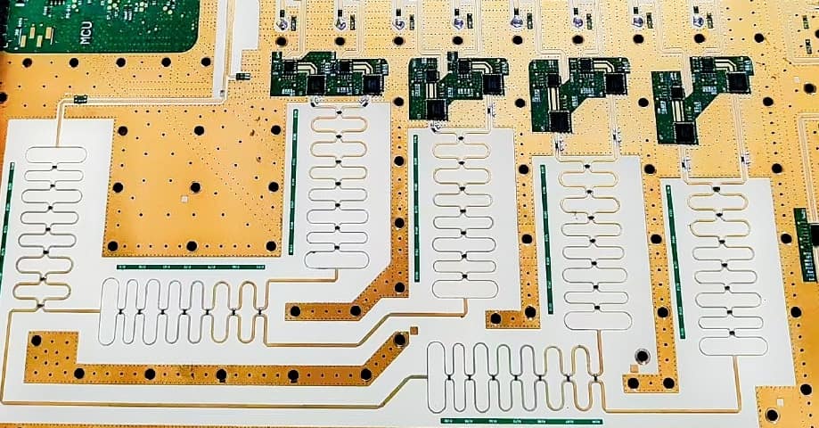
What kind of PCB design is suitable for snake routing
There are different application for snake routing:
If snake routing used in the computer PCB board, it mainly plays the role of filter inductance and impedance matching to improve the anti-interference ability of the circuit. The snake routing in the computer PCB board is mainly used in some clock signals, such as PCI CLK, agpcik, IDE, DIMM and other signal lines.
If snake routing used in the common PCB board,In addition to filtering inductance, it can also be used as the inductance coil . For example, 2.4G walkie talkie is used as inductance.
For those strictly equal wiring length of signals . The equal line length of high-speed digital PCB is to keep the delay difference of each signal within a range and make the data read by the system in the same cycle.
For example, there are 13 hublinks in the Intel hub architecture, with a frequency of 233MHz,they must be strictly equal in length to eliminate the hidden danger caused by time delay. Generally, the delay difference is not more than 1 / 4 of the clock cycle, and the line delay difference per unit length is also fixed.
The delay is related to the line width, line length, copper thickness and board structure, but the long line will increase the distributed capacitance and distributed inductance and degrade the signal quality. Therefore, the clock IC pins are commonly connected and terminated, but the snake wiring routing does not play the role of inductance. On the contrary, the inductance will phase shift the higher harmonic in the rising edge of the signal, resulting in the deterioration of signal quality. Therefore, the spacing of snake routing lines is required to be at least twice the line width. The smaller the time of the signal, the more influence caused by the distributed capacitance and distributed inductance.
Snake routing acts as a distributed parameter LC filter in some special circuits.
How to consider the impact of PCB wiring on analog signal transmission, and how to distinguish the noise from the signal transmission caused by wiring or operational amplifier devices?
It is difficult to distinguish. We can only use reasonable design to avoid additional noise from PCB wiring.


