Overview of DFM Technical Requirements for PCB Process
Design for Manufacturability (DFM) optimizes designs for the manufacturing process, making it an essential component of concurrent engineering. By considering factors such as manufacturability and assembly requirements early in the design phase, DFM streamlines production, bridges CAD-CAM communication, and enhances product reliability. Here, we cover general technical requirements for DFM in PCB manufacturing.
I. General Requirements
- Standard Requirements
These general guidelines for PCB design ensure alignment between PCB design and manufacturing, facilitating CAD-CAM communication. - Production Priority
Our company prioritizes production based on design drawings and documentation, ensuring alignment with processing files.
II. PCB Materials
- Substrate
Commonly, PCB substrates are FR4 epoxy glass cloth copper-clad laminates, including single-sided boards. - Copper Foil
- Purity: Electrolytic copper should have 99.9% purity or higher.
- Thickness: Standard double-layer board copper thickness should be ≥35µm (1oz). Specify any special requirements in documentation.
III. PCB Structure, Size, and Tolerance
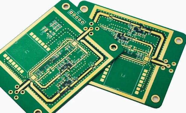
- Structure
- Design elements that define the PCB structure should be represented on the Mechanical 1 layer (preferred) or Keep-out layer.
- SLOT holes or hollow spaces should be defined on the Mechanical 1 layer.
- Board Thickness and Dimension Tolerance
- Board thickness tolerance should align with design specifications.
- Dimension tolerance is ±0.2mm unless otherwise specified (excluding V-CUT products).
- Flatness (Warpage) Tolerance
Comply with drawing requirements; follow default specifications if unspecified.
IV. Printed Conductors and Pads
- Layout
- Printed Conductors: Width and spacing follow the design drawing. Adjustments are made as needed to enhance manufacturability, especially for single-sided boards.
- Spacing and Width Recommendations: For single and double-sided boards, we recommend a VIA inner diameter ≥0.3mm, outer diameter ≥0.7mm, line spacing ≥8mil, and line width ≥8mil.
- Wire Width Tolerance
Our standard wire width tolerance is ±15%. - Grid Processing
- Use a grid pattern for large copper areas to prevent surface blistering and bending during soldering.
- Grid spacing should be ≥10mil, and line width should be ≥10mil.
- Thermal Pad Processing
Thermal pads are recommended in large grounding areas to prevent false soldering by reducing heat dissipation.
V. Hole (HOLE) Specifications
- Metallization and Non-metallization (PTH and NPTH)
- Non-metallized holes include unplated holes defined in design software or those labeled as NPTH.
- Unless specified otherwise, component holes, mounting holes, and vias are metallized.
- Hole Diameter and Tolerance
- Component and mounting holes default to finished hole diameter sizes with ±3mil tolerance.
- For VIA holes, positive tolerance is capped at +3mil.
- Copper Plating Thickness
The copper plating in metallized holes should average at least 20µm, with no part thinner than 18µm.
VI. Solder Mask
- Coating and Adhesion
Solder mask should cover all PCB areas except pads, MARK points, and test points. FILL or TRACK pads should be represented graphically on the solder mask layer to indicate tinning. - Thickness and Adhesion Standard
The solder mask thickness must meet Class 2 of the IPC-A-600F standard.
VII. Characters and Etching Marks
- Text Requirements
- Character height should be 30mil, width 5mil, with spacing >4mil.
- Etched metal characters require sufficient spacing to avoid electrical bridging.
- Text Placement on Pads
No silk-screen text should overlap PADs to prevent false soldering.
VIII. Layers and MARK Point Processing
- Layer and Orientation
- Double-sided boards assume the Top layer as the front view.
- Single-sided boards with the signal layer on the Top layer represent a front view; with the signal layer on the Bottom layer, it represents a rear view.
- MARK Points
- Place MARK points with a diameter of 1.0mm for SMT panels. For additional process edge marks, add a 1.5mm arc on the solder mask layer.
IX. V-CUT Specifications
- Panelization and Conductor Spacing
Ensure a 0.5mm spacing from the conductor on both sides of the V-CUT line, or 0.25mm for individual boards. - V-CUT Depth and Tolerance
V-CUT depth should leave a residual thickness of 1/3 of the board thickness, adjustable to specific customer requirements.
X. Surface Treatment Process
By default, our surface treatment process uses hot air leveling (HAL) with 63% tin and 37% lead unless specified otherwise.
As a leading PCB manufacturer, members of our printed circuit board (PCB) design service team are practical partners working with you on every project and can help you achieve your goals at any time. They can complement your engineering expertise, which helps speed up time to market, reduce the time from concept to production, and ensure that quality is integrated into the manufacturing process to maximize your profits.


