Overview of Copper Foil for PCB Laminates
Copper foil used in the PCB industry is more complex than you might think. Copper is both an excellent conductor of electricity and an excellent conductor of heat, making it an ideal conductor for most PCB applications. Copper foil has many other properties that are important for engineers to understand.
The copper foil used in the PCB industry generally comes in two types: rolled annealed copper (RA) or electrolytic (ED). The manufacturing process of rolled copper foil starts with pure copper billets, which are continuously rolled and reduced to the desired thickness. ED copper foil is manufactured using an electroplating process, in which copper is plated on a rotating titanium drum. As the titanium drum rotates, copper ions are gradually deposited to form copper foil. The rotation speed of the titanium drum directly affects the thickness of the copper foil. After the copper foil is made, both RA and ED copper foil need to go through multiple processes.
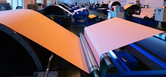
Copper foil has a variety of processing methods
Copper foil is treated in many ways for many reasons. Some of these treatments are passivation treatments designed to ensure that the foil does not oxidize before use. Other foil treatments are designed to promote good chemical adhesion to certain resin systems (such as PPE and PTFE). Due to differences in resin systems, the material reacts differently to various treatments. Because each resin system has different bonding characteristics, some treatment/resin combinations will work better than others to achieve good adhesion. There are also some foil treatments that ensure proper bonding under high temperature conditions. There are still other treatments that form a reliable bonding surface to ensure long-term reliability at high temperatures, etc.
For rigid PCB applications, ED copper foil is the most commonly used, but RA copper foil is also used. Generally speaking, RA copper foil is more expensive than ED copper foil. RA copper foil is generally not used unless some characteristics of RA copper foil are more advantageous for the application. The manufacturing process of RA copper foil makes its surface very smooth, and copper foil with a smooth surface has low insertion loss , so it is well suited for high-frequency and ultra-high-speed digital applications. As a product of a unique manufacturing process of copper foil, RA copper foil also features an in-plane crystal structure, which is very beneficial for applications that require circuit bending. Correspondingly, there is a technical disadvantage of RA copper foil that is also related to this crystal structure, namely the etching of tiny circuit features. Of course, specific etching of RA copper foil can be used to overcome this problem to a certain extent.
ED copper foil is widely used throughout the PCB industry. There are many different types of ED copper foil, which are usually classified by surface roughness and/or treatment. IPC classifies ED copper foil into different categories based on the roughness of the copper foil, including LP (low profile), VLP (very low profile) and HVLP (very low profile).
There are many ways to measure copper foil roughness
There are many ways to measure copper foil roughness, and the results can be confusing because of the differences in the methods. Generally speaking, there are two methods for measuring roughness: contact measurement and non-contact measurement. Contact measurement uses a physical probe (i.e., a stylus) to measure the peaks and valleys on the copper foil surface. Non-contact measurement generally determines the peaks and valleys on the copper foil surface through reflected light or laser measurement.
Contact profilometers are less accurate due to the varying stylus tip sizes and are unable to detect the depth of ultra-narrow roughness valleys. Also, the stylus may simply “plow” over the highest point without accurately measuring it. Experienced engineers are familiar with these issues and can often make minor adjustments to mitigate accuracy issues. In general, however, non-contact profilometers are generally more accurate than contact profilometers for fine-grain copper foil.
There are many ways to describe the surface roughness characteristics of copper foil
There are many ways to describe the surface roughness characteristics of copper foil. PCB manufacturing engineers usually use Rz value to describe it. Rz represents the peak-to-valley value measured on multiple straight lines on a sample area. If the Rz value is measured as an area (rather than a straight line), then Rz will be named Sz. The Sz value has the same meaning as the Rz value. For high-frequency or high-speed digital (HSD) design engineers, the Rq or Sq parameter value of copper foil is usually required. Rq/Sq represents the root mean square value of the surface roughness of copper foil measured on multiple samples. Through the classic electromagnetic model, it is found that the Rq/Sq parameter can better reflect the impact of copper foil roughness on the performance of RF or HSD, and its electromagnetic model can better match the performance of the actual circuit.
There is another characteristic description of copper foil surface roughness that is of interest in modeling: the surface area index (SAI), also known as the surface area ratio. It is defined as the ratio of the surface area of roughness in the scanned area to the ideal flat area of the area. This roughness value can be used for specific electromagnetic model simulations, so that its simulation results can show excellent matching and accuracy with the actual circuit over an ultra-wide bandwidth.

