Multilayer PCBs: Overview, Manufacturing, and Design Considerations
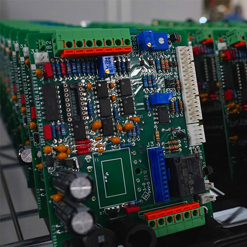
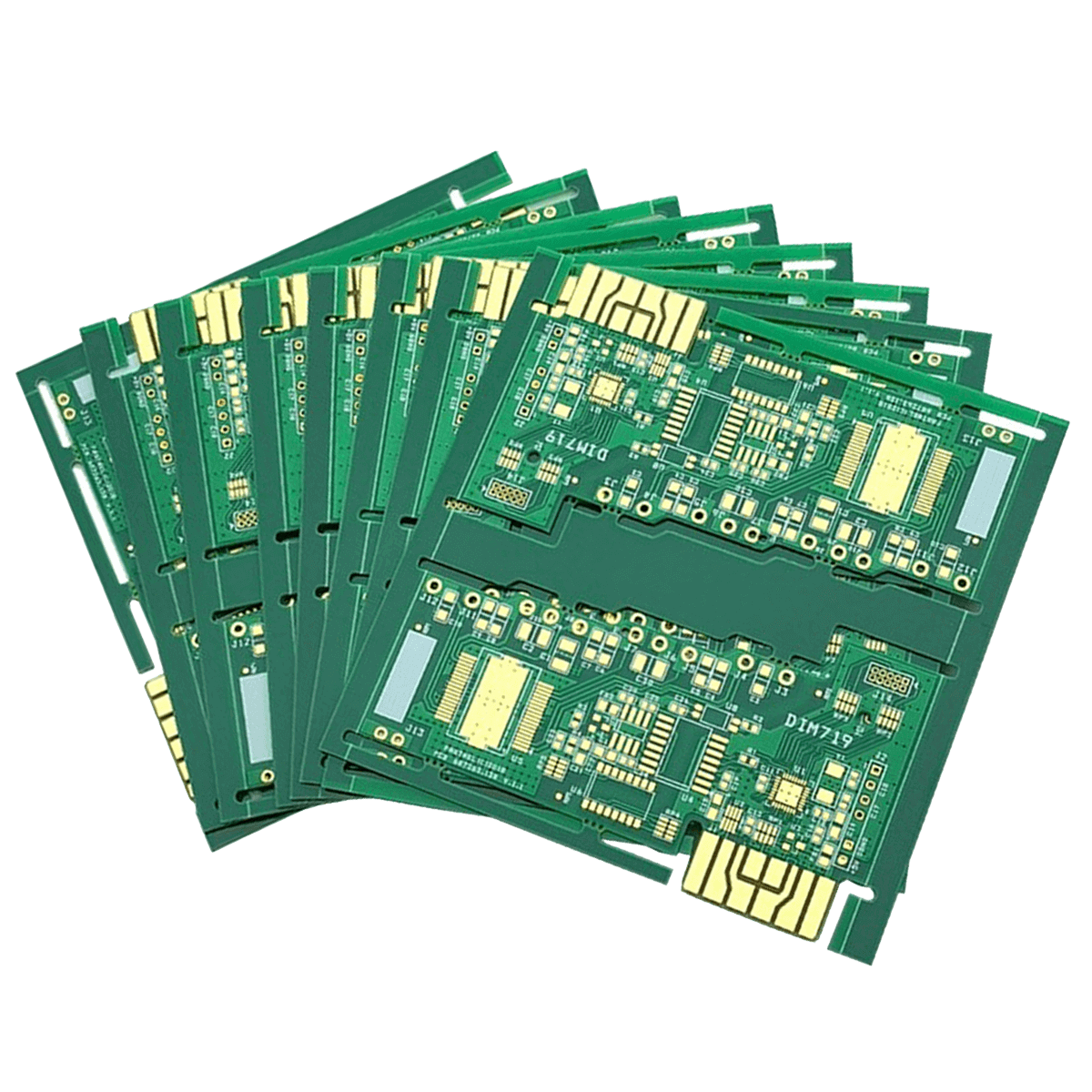
Multilayer Printed Circuit Boards (PCBs) or Multilayer Boards (MLBs) feature more than two copper layers, interconnected using copper-plated holes. These holes may include NC vias, laser microvias, through-holes, buried, or blind vias. The layers consist of copper foil, prepreg (PP), or adhesive materials and are pressed together under high temperature and pressure. This process removes air and cures the thermosetting adhesives, forming a cohesive multilayer PCB.
Layer Count Options for Multilayer PCBs
Multilayer PCBs are versatile and available in various formats, including rigid, flex, rigid-flex, and metal-core types. The following layer counts are typical for each type:
- Rigid Multilayer PCBs: 4, 6, 8, up to 30 layers.
- Flex Multilayer Circuits: 3 to 8 layers.
- Rigid-Flex Multilayer PCBs: 2 to 20 layers.
- Metal-Core Multilayer Boards: Up to 4 layers.
Manufacturing Process for Multilayer PCBs
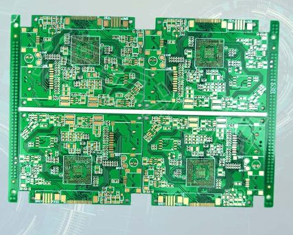
Fabricating multilayer PCBs involves precise attention to detail to align all layers accurately. Here’s an overview of the manufacturing steps:
- Material Preparation
Layers are prepared and loaded as “chapters” of up to 10 unpressed panels. Each “book” of chapters is separated by steel plates and compressed using hydraulic presses. - Pressing Process
The pressing process melts and solidifies the prepreg material, ensuring that the layers are securely bonded. Polyimide material may require special modifications compared to standard FR4 processing.
Multilayer PCB Stack-Up Design
Effective stack-up design is crucial for optimizing the performance, cost, and reliability of multilayer PCBs. Consider the following factors:
- Performance Requirements
Material choice impacts operational parameters such as impedance. Consult your PCB manufacturer to determine the best materials for your application. - Cost Optimization
Materials, layer counts, and configurations affect manufacturing costs. Collaborate with your supplier to identify cost-effective solutions. - Density and Routing
High-density designs require careful planning. Adding layers post-layout can be costly and time-consuming. - Circuitry Needs
Sensitive signals may need specific configurations, such as stripline layers with additional ground planes. Analog and digital areas should have separate grounding to avoid interference.
PCB Layout: Placement and Routing in Multilayer Boards
Designing multilayer PCBs demands a 3D perspective. Key considerations include:
- Component Placement
Avoid placing noisy components above sensitive internal routing. - Internal Routing
Leverage inner layers for dense routing, reserving surface layers for sensitive or direct connections. - Signal Integrity
Avoid crossing split ground planes to prevent noise issues. Maintain proper spacing for differential pairs and controlled impedance routing.
Fabrication Documentation and Outputs
To ensure successful manufacturing, detailed documentation is essential:
- Fabrication Drawings
Include stack-up details and notes for the PCB assembly process. - Gerber Files
Generate files for all layers, including additional ones for the multilayer design.
Design for Manufacturability (DFM)
Optimize your multilayer PCB design by adhering to manufacturing standards:
- Copper Clearance: Maintain at least 10 mil clearance from the edge, preferably 20 mil.
- Via Clearance: Ensure at least 15 mil clearance, preferably 20 mil.
- Thermal Relief Pads: Use ties with a minimum of 8 mil width.
Avoiding Bow and Twist in Multilayer PCBs
Bow and twist issues often arise from asymmetric or unconventional designs:
- Symmetric Stack-Ups: Maintain symmetry in layer thickness to balance stress and minimize deformation.
- Odd Layer Counts: Odd numbers like 3, 5, or 7 layers may cause stress imbalances. Use even layers wherever possible.
- Consistent Layer Thickness: Avoid variable thicknesses in build-ups to reduce deformation risks.
Conclusion
Multilayer PCBs are essential for modern electronics, enabling compact, high-performance designs. Understanding the manufacturing and design intricacies ensures a successful and cost-effective outcome. By working closely with your PCB supplier and adhering to best practices, you can achieve reliable, high-quality multilayer PCB solutions


