


Optimizing PCB Trace Thickness vs. Current Capacity
The relationship between PCB trace thickness and current capacity is a critical aspect of PCB design. Properly sizing traces ensures that they can handle the required current without overheating, which is essential for the reliability and functionality of the circuit. This article explores the key considerations for selecting trace thickness, the impact of copper weight, and methods for calculating current capacity, along with design strategies for high-current applications.
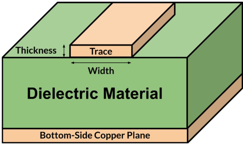
Key Considerations for Trace Thickness Selection
When designing PCB traces, several factors influence the choice of trace width and thickness to ensure adequate current capacity and thermal management:
1. Cross-Sectional Area
- The cross-sectional area of a trace determines its current-carrying capacity. Wider and thicker traces can handle higher currents.
- Formula: Cross-sectional area (A) = Trace thickness (T) × Trace width (W) × 1.378
(Where T is in ounces per square foot, W is in mils, and 1.378 is a conversion factor.)
2. Trace Positioning
- External Layers: Traces on outer layers dissipate heat more effectively than those on inner layers due to exposure to air.
- Internal Layers: Inner layer traces have reduced heat dissipation, requiring wider or thicker traces for the same current capacity.
3. Trace Length
- Longer traces experience higher resistance, leading to increased heat generation. Wider traces may be necessary to maintain signal integrity and prevent overheating.
4. Copper Thickness
- Copper thickness is typically measured in ounces per square foot (oz/ft²). Common thicknesses include 0.5 oz, 1 oz, and 2 oz.
- 0.5 oz = 0.7 mils = 0.018 mm
- 1 oz = 1.4 mils = 0.035 mm
- 2 oz = 2.8 mils = 0.070 mm
- Thicker copper reduces resistance and increases current capacity but adds cost and complexity to manufacturing.
5. Temperature Rise
- The allowable temperature rise (ΔT) is a key parameter. A typical target is 10–20°C to ensure reliability.
- Higher temperature rises allow for narrower traces but increase the risk of thermal damage.
IPC Standards for Current Capacity
The IPC-2152 and IPC-2221 standards provide guidelines for determining trace width and current capacity:
IPC-2152
- Offers detailed models for evaluating temperature rise based on trace location, copper thickness, and board material.
- Accounts for real-world conditions, such as thermal conductivity of the PCB substrate.
IPC-2221
- Provides general design rules, including trace width vs. current capacity tables.
- Includes recommendations for electrical spacing, insulation, and other design factors.
Calculating Maximum Current Capacity
To calculate the maximum current a trace can carry, use the following steps:
- Calculate Cross-Sectional Area (A):A=T×W×1.378A=T×W×1.378
- TT = Trace thickness (oz/ft²)
- WW = Trace width (mils)
- AA = Cross-sectional area (mils²)
- Determine Maximum Current (I<sub>MAX</sub>):IMAX=k×(A)b×(ΔT)cIMAX=k×(A)b×(ΔT)c
- kk, bb, and cc are constants (for inner layers: k=0.048k=0.048, b=0.44b=0.44, c=0.725c=0.725).
- ΔTΔT = Temperature rise (°C).
Design Strategies for High-Current Applications
For applications requiring high currents (e.g., motor control, power inverters, electric vehicles), consider the following approaches:
1. Increase Copper Weight
- Use 2 oz or 3 oz copper to reduce resistance and increase current capacity.
- Thicker copper is more expensive and may require adjustments to the manufacturing process.
2. Widen Traces
- Wider traces provide a larger cross-sectional area, enabling higher current capacity.
- Ensure adequate space on the PCB for wider traces.
3. Use Multiple Layers
- Distribute high-current traces across multiple layers and connect them with vias (via stitching) to increase current capacity without increasing trace width.
4. Employ Copper Busbars
- For extremely high currents (>100A), use copper busbars soldered to the PCB. Busbars provide a low-resistance path for current flow.
Example: Maximum Current Capacity for 2 oz Copper
The table below shows the maximum current capacity for 2 oz copper traces with a 10°C temperature rise:
| Maximum Current (A) | Inner Layer Trace Width (mils) | Outer Layer Trace Width (mils) |
|---|---|---|
| 2 | 20.03 | 19.95 |
| 4 | 66.86 | 66.59 |
| 6 | 135.34 | 134.78 |
| 8 | 223.21 | 222.28 |
| 10 | 329.05 | 327.68 |
Optimizing PCB trace thickness and width for current capacity is essential for ensuring reliable and efficient circuit performance. By considering factors such as copper weight, trace positioning, and temperature rise, and leveraging IPC standards and calculation tools, engineers can design PCBs that meet both electrical and thermal requirements. For high-current applications, strategies like increasing copper weight, widening traces, and using multiple layers or busbars can help achieve the necessary performance without compromising reliability.
KKPCB provides global customers with one-stop services from PCB layout, prototype PCB proofing, PCB manufacturing, PCBA processing (including SMT and DIP), PCBA testing, PCBA product assembly and outbound packaging. You could provide a Gerber file or BOM list to us, we will offer the finished PCB products or PCB assembly which are satisfied with you.