One-stop PCB Manufacturing and PCB Assembly solutions Manufacturer
- Mon - Sat: 8.00 am - 7.00 pm
- sales@kkpcb.com
One-stop PCB Manufacturing and PCB Assembly solutions Manufacturer
Over 10 years we help companies reach their financial and branding goals. Engitech is a values-driven technology agency dedicated.
411 University St, Seattle, USA
engitech@oceanthemes.net
+1 -800-456-478-23
KKPCB conducts research on special processing technologies such as ordinary double-sided boards, thick copper circuit boards, high-frequency circuit boards, HDI circuit boards, rigid-flexible circuit boards, FPC flexible boards, buried blind hole circuit boards, and IC carrier boards. Provides PCB design, PCB layout, PCB prototyping and PCB assembly services.
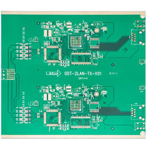
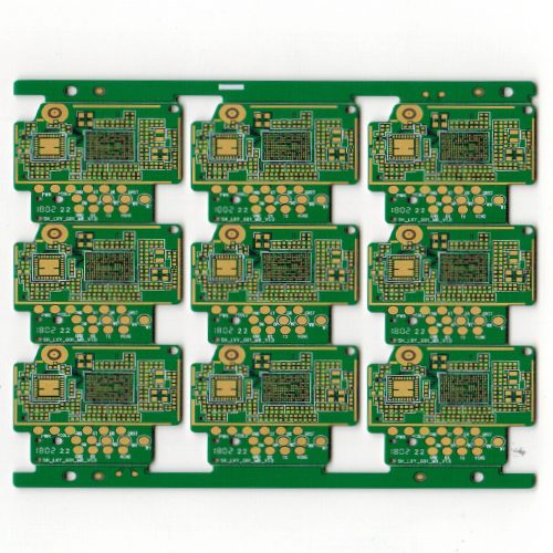
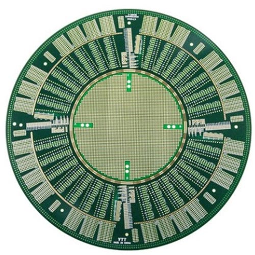
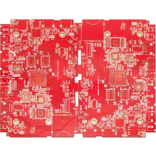
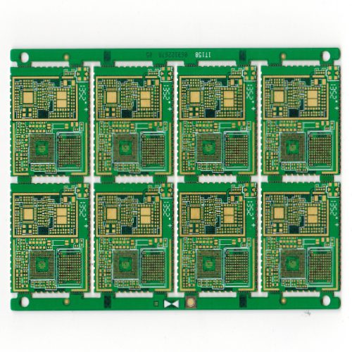
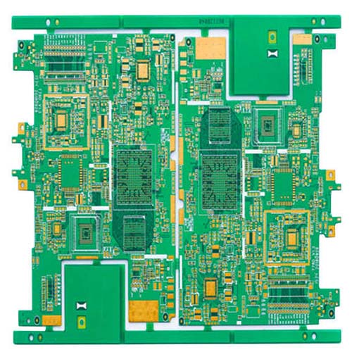
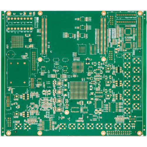
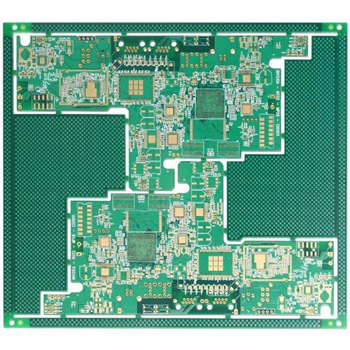
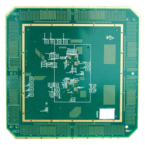
Multilayer board refers to a PCB that has more than three conductive pattern layers and is laminated with insulating materials between them. With the development of electronic technology to high-speed, multi-function, large capacity, and portable low-consumption direction, the application of multi-layer PCB is more and more widely, and its layer number and density are also higher and higher, and the corresponding structure is also increasingly complex. The production of multilayer PCB has become the most important part of the whole PCB industry. At present, the average number of layers of KKPCB has reached 8-20 layers, can up to 64 layers, which has reached a high level in terms of inner layer manufacturing ability and laminating ability. The emergence of multi-layer board technology is a major development of the PCB industry, which makes the whole PCB technology advance by leaps and bounds.
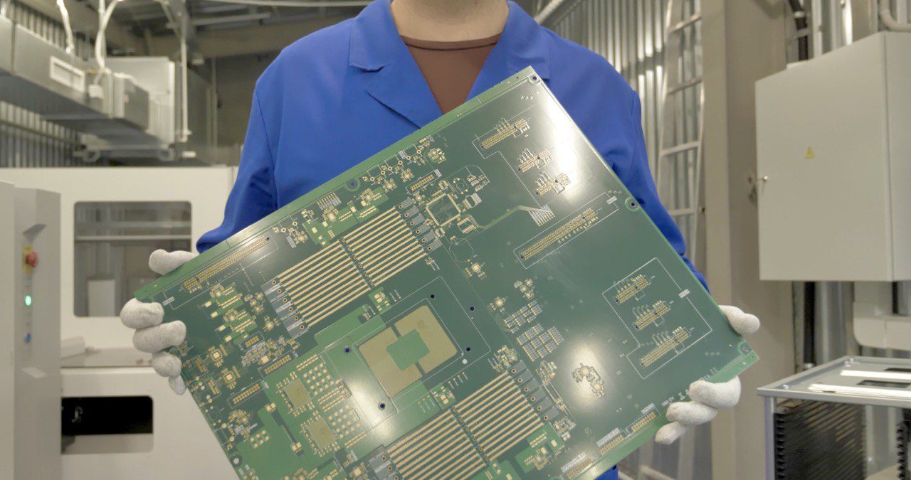
KKPCB is very good at multilayer PCB fabrication and prototyping. The manufacturing process of ordinary multilayer PCB is mainly based on lamination technology. Multi-layer lamination is an important process in PCB manufacturing. KKPCB has been producing multilayer PCBs for over 20 years. Over the years, we have seen all types of multilayer constructions from various industries, answered all types of multilayer questions, and solved all types of problems with multilayer PCBs.
The control of lamination quality is becoming more and more important in multilayer PCB fabrication. Therefore, it is necessary to ensure multilayer laminate quality, need to have a good understanding of multilayer laminate technology. According to the processing practice for many years, KKPCB summarizes how to improve the laminating quality of multilayer boards as follows.
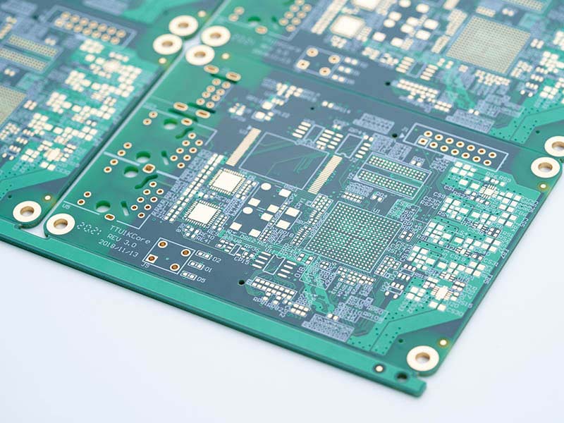
1. The thickness of the core board should be selected according to the total thickness requirements of the multilayer board. The thickness of the core board should be consistent and the deviation is small.
2. There should be a certain distance between the overall dimension of the core board and the effects unit, that is, the distance from the effective unit to the edge of the board should be on the premise of not wasting materials try to keep more space.
3. Design of positioning hole. In order to reduce the deviation between layers, attention should be paid to the design of positioning holes in multi-layer boards: 4-layer multilayer only needs to be designed more than 3 positioning holes can be used for drilling. For multi-layer boards with more than 6 layers, in addition to designing positioning holes for drilling, it is also necessary to design more than 5 overlapping positioning rivet holes and more than 5 positioning holes for the tool plate for rivets.
4. The inner core board shall be free from the open, short, open circuit, oxidation, clean board surface, and no residual film.
5. Meet the requirements of PCB users, select the appropriate PP and copper foil configuration. For 4-ply laminates, 7628, 3313 or 7628 + 1080, 7628 + 2116 can be used etc. 1080 or 2116 is the main choice of PP for multilayer boards with more than 6 layers, and 7628 is mainly used to increase the thickness of the dielectric layer. At the same time, PP requires symmetrical placement to ensure mirror effect and prevent plate bending.
6. Inner core board pretreatment process. The treatment process of the inner layer core board includes the black oxidation process and browning treatment process. The oxidation treatment process is to form a black oxide film on the inner copper foil, the thickness of the black oxide film is 0.25-4.50mg/cm2. The browning process (horizontal browning) is to form an organic film on the inner copper foil.
The functions of the inner laminate treatment process are as follows:
a. Increasing the surface ratio of inner copper foil and resin can enhance the adhesion between them.
b. The effective wettability of the melt resin to copper foil is increased so that the flowing resin has sufficient ability to penetrate into the oxide film and show a strong grip after curing.
c. It can prevent the decomposition of dicyandiamide in liquid resin at high temperatures and influence on the copper surface.
d. It can improve the acid resistance and prevent the PINK ring in the wet process.
7. The organic matching of lamination parameters, the control of multi-layer board lamination parameters mainly refers to the organic matching of lamination “temperature, pressure, and time”. How to determine the lamination temperature, pressure, and time software parameters is the key technology for multilayer laminate processing.
Copper foil
Basic material composed of the conductive pattern
Core board
A framework of the circuit board, double-sided copper clad board, which can be used for double-sided board production.
Prepreg
The indispensable material for multilayer board production and the adhesive between core board and core board plays an insulating
role at the same time.
Various types of most commonly used FR-4 prepreg materials
| Material name | Material type | Original thickness (um) |
| FR4 | 7628 | 193 |
| 1506 | 150 | |
| 2116 | 122 | |
| 3313 | 99 | |
| 1080 | 74 | |
| 106 | 60 |
Difference between single layer and multilayer PCB
Compared with a double-layer board, the multilayer PCB has greatly improved electromagnetic compatibility.
For example, in a four-layer board, the middle layer is used as a power layer and a ground layer, and the benefits of doing so are as follows,
1. The inductance of the power wire and ground wire is greatly reduced, thus reducing the noise voltage
2. The power supply layer and ground layer form a large distributed capacitor, which provides a good high-frequency decoupling effect for the power supply, thus reducing the noise on the power cord.
3. Independent power and ground layer can minimize the area of all signal loops
4. PCB multilayer board is the trend of the circuit board industry, the circuit board industry is developing toward a smaller size, the smaller the hole, the thinner the thickness, the larger the number of layers, the smaller the line width and spacing, and so on.
5. Many high-precision high-tech electronic products are required multilayer PCB boards to achieve functions, the ordinary double-sided board simply cannot replace them.
According to usage, it can be divided into
According to hardness, it can be divided into
According to the conduction state of the hole, it can be divided into
Classification by substrate
As mentioned above, multilayer PCB can be used in civil, industrial, and military fields. Multilayer PCB can be used for any purpose.
For many industries, multilayer PCB has become the first choice for various applications. This preference is largely due to the continuous promotion of mobility and functionality by all technologies. Multilayer PCB is a reasonable step in this process, which can reduce the size and realize more functions. As a result, they have become quite common, including:
KKPCB is widely known as a professional PCB supplier in the electronic manufacturing industry. We have years of experience in the multilayer PCB, HDI PCB segments. KKPCB further expands its range of products including rigid, rigid-flex, HDI, any layer, Flex, large-size, embedded, RF, LED, backplane, the metal substrate, a ceramic substrate, IC structure, high-frequency, heavy copper. High quality and high reliability.
In designing Multilayer PCB, one of the most important things is to plan the stack of Multilayer PCB to achieve the best performance of the product. The bad design of the substrate and improper selection of materials will reduce the electrical performance of the signal transmission, increase emission and crosstalk, and make the product more vulnerable to external noise. These problems can lead to intermittent operation because timing glitches and interference can significantly reduce product performance and long-term reliability.
In contrast, a properly constructed PCB board can effectively reduce electromagnetic radiation, crosstalk and improve signal integrity, thus providing a low inductance distribution network.
According to experience, compared with a double-sided PCB board, the radiation of a four-layer board will be reduced by 15 dB.
When selecting a multilayer stack, we should consider the following factors:
1) Below the surface of the component (the second layer) is the ground plane, which provides the components shielding layer and provides the reference plane for the component surface wiring;
2) All signal layers shall be adjacent to the ground plane as far as possible;
3) Try to avoid two signal layers directly adjacent;
4) The main power supply should be adjacent to its corresponding ground as far as possible;
5) In principle, a symmetrical structure design should be adopted. The meaning of symmetry includes: thickness and type of dielectric layer, the thickness of copper foil, and figure
6) The distribution type (large copper foil layer, circuit layer) is symmetrical.
4 Layer PCB lamination
A typical four layers PCB laminate is shown below.

4 Layer PCB stack
Four layers of PCB are usually seen stacked evenly. That is, four evenly spaced layers with the plane at the center. While this does make the board symmetrical, it does not help EMC.
In addition, another common mistake is to make the plane tightly coupled to the large dielectric layer and plane between the center and the signal. This certainly produces good interplane capacitance, but it also doesn’t help signal integrity, crosstalk or EMC – that’s why we chose to use 4-layer PCBs on two layers.
To improve the EMC performance of the capacitor, it is better to put the signal layer as close as possible to the plane (< 10 mil), and use a large core (~ 40 mil) between the power supply and the ground plane to maintain the overall substrate thickness 62 mil. Close tracking of planar coupling will reduce crosstalk between traces and allow us to keep impedance at an acceptable value.
6 Layer PCB stack
The six-layer PCB board is basically a four-layer board, adding two additional signal layers between the planes. This greatly improves EMI because it provides two buried layers for high-speed signals and two surface layers for routing low-speed signals. The signal layer should be placed very close to the adjacent plane and the plate thickness (62 mil) should be composed of a thicker central core. There is always a trade-off between trace impedance, trace width and prepreg/core thickness. Differential pairs are becoming more and more common in high-speed design. Noise is reduced by using differential mode signals.

6 Layer PCB stack& 8 Layer PCB stack
To improve EMC performance, add two more planes in the six stack. It is recommended not to have more than two adjacent signal layers between the planes as this creates impedance discontinuities (signal layer impedance difference of ~ 20 Ohm) and increases crosstalk between these signal layers.
In the following case, two plane layers are added to the center of the substrate. This allows tight coupling between the central planes and isolates each signal plane, thereby reducing coupling and significantly increasing crosstalk. This configuration is usually used for high-speed signals in DDR2 and DDR3 designs where crosstalk due to tight wiring is a problem.
10 Layer PCB stack
When six wiring layers and four planes are required, ten layer boards should be used – and EMC deserves attention.
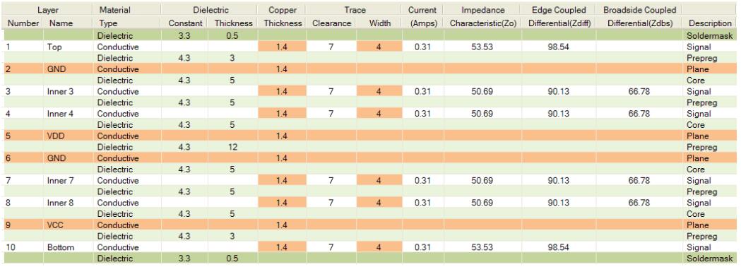
A typical 10 layer overlay is shown above. This superposition is ideal because of the tight coupling of the signal and returns plane, the shielding of the high-speed signal layer, the presence of multiple ground planes, and the symmetry of tightly coupled power/ground at the center of the circuit board. High-speed signals are usually routed on signal layers buried between planes (in this case, layers 3-4 and 7-8). However, care should be taken to route these signals correctly. Other, avoid coupling (crosstalk) between adjacent layers.
12 layer PCB stack
12 layers are the maximum number of layers that can be easily made in 62mil thick PCB. Occasionally you’ll see 14 to 16 layers of boards made into 62mil thick boards, but the number of manufacturers that make them is limited to those who can make HDI boards. The above twelve stacked layers provide shielding on six inner layers.
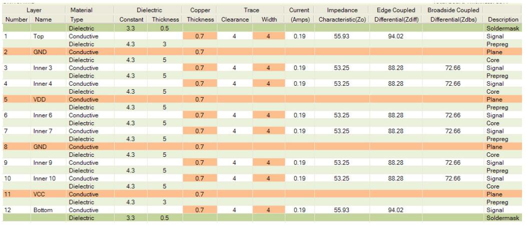
12 Layer PCB stack &14Layer PCB stack
When eight routing (signal) layers are required, a special critical shield is required to use the 14 layer overlay below. Layers 6 and 9 provide isolation for sensitive signals and 3, 4 and 11, 12 provide shielding for high-speed signals.
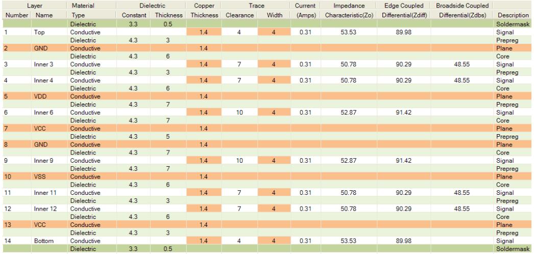
14 Layer PCB stack & 16 Layer PCB stack
16 Layer PCB provides ten layers of wiring, which are usually used in extremely dense designs. Typically, you will see a 16 layer PCB where the routing technology used in EDA applications cannot route the design to completion. “If it doesn’t route – just continue adding layers. “. Although this is a common saying, it is not a good practice.
If the board cannot complete the route, then there may be many reasons. Bad placement is often. Open the routing channels, reduce the number of crosses in the rat network, place vias on the 25 mil grid to allow routing and help routers as much as possible.
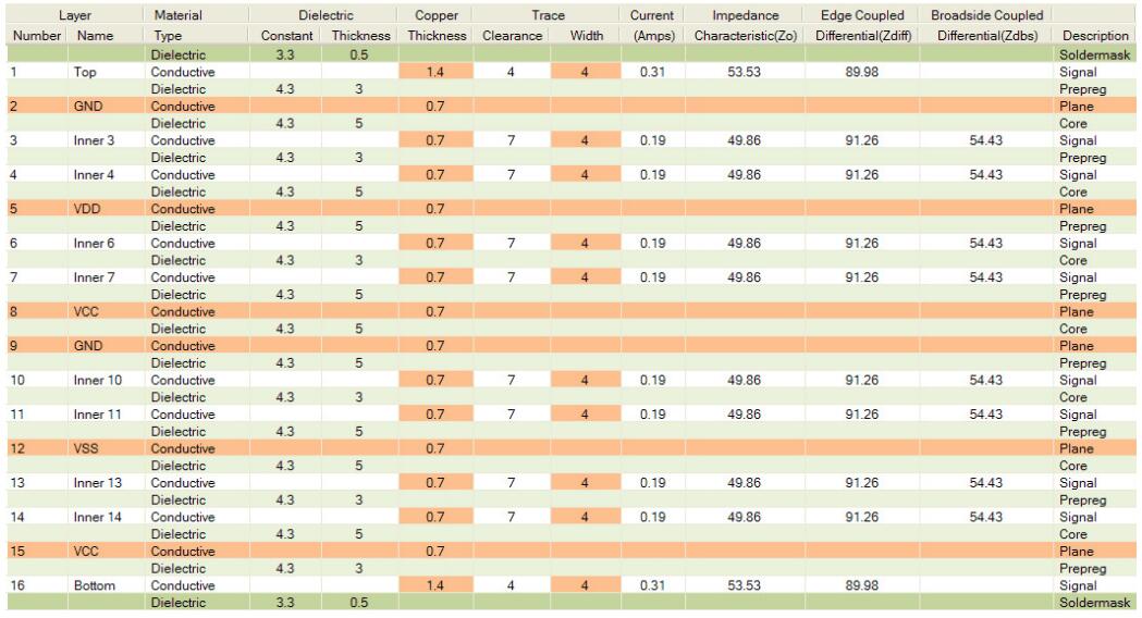
16 Layer PCB stack
The number of layers that can be manufactured is not actually limited to Multilayer PCB (please check the manufacturer’s function first). Of course, as the number of layers increases, the PCB thickness increases to accommodate the minimum thickness of the material used. The aspect ratio (board thickness and minimum hole size) must also be considered. Generally speaking, the thickness of 100 Mil material is 10:1. For example, a 200 mil thick substrate has a minimum hole size of 20 mils.
The technical rule is based on the minimum spacing of SMT components used, which is basically the maximum routing, clearance and through-hole allowed while minimizing PCB manufacturing costs. Complex high-speed designs using a ball grid array (BGA) usually require 4 / 4 mil (routing/gap) and 20 / 8 mil (PAD/hole) via technology. However, if you can, use smaller sizes, which will reduce costs and increase manufacturing output.
Once these rules are established, the required characteristic impedance (Zo) and differential impedance required stack (Zdiff) are calculated according to the component datasheet. Typically, 50 ohm Zo and 100-ohm Zdiff are used. Keep in mind that lower impedances increase the di / dt and significantly increase the absorbed current (which is detrimental to the PDN), and higher impedances generate more EMI and make the design more susceptible to external influences. Therefore, a good Zo range is 50-60 ohm.
The total number of layers required for a given design depends on the complexity of the design. Factors include the number of signaling networks that must break through from BGA; the number of power supplies required by BGA; component density and package type.
Experienced designers will know about it after a while, but checking that there are enough layers is a good way to automatically adjust the board. If not adjusted, the router needs to complete at least 85% of the routing to indicate that the selected stack is routable. You may need to reevaluate the placement several times for the best results.
A multilayer PCB (Printed Circuit Board) is composed of three or more layers of conductive material (such as copper foil) and insulating material (such as FR4) stacked alternately. Its structure typically includes:
Advantages of Multilayer PCBs
Multilayer PCBs are widely used in the following fields:
Multilayer PCBs (Printed Circuit Boards) differ from regular (single-layer or double-layer) PCBs in several key aspects, including their structure, complexity, capabilities, and applications. Here are the main differences:
Structural Differences
Number of Layers:
Interconnections:
Complexity and Design
Design Complexity:
Signal Integrity:
Capabilities
Electrical Performance:
Component Density:
Applications
Manufacturing Considerations
Cost:
Manufacturing Process:
In summary, multilayer PCBs provide greater design flexibility, higher performance, and the ability to handle more complex and compact designs compared to single-layer and double-layer PCBs, making them suitable for advanced and high-demand applications.
The production of multilayer PCBs involves using various sheet materials, primarily for the substrate and dielectric layers. Here are the main types of sheet materials used:
Substrate Materials
FR4 (Flame Retardant 4)
Polyimide
PTFE (Polytetrafluoroethylene)
CEM-1 and CEM-3 (Composite Epoxy Material)
Dielectric Materials (Prepreg and Core)
Advanced Dielectric Materials
Rogers Materials
BT Epoxy (Bismaleimide-Triazine Epoxy)
Teflon (PTFE)
Specialized Materials
Ceramic Substrates
Metal Core PCBs (MCPCBs)
The choice of sheet materials depends on the specific requirements of the PCB, including electrical performance, thermal management, mechanical strength, cost, and application-specific needs.
Testing multi-layer PCBs (printed circuit boards) is essential to ensure their reliability and functionality. Here are the main methods for testing multi-layer PCBs:
1. Visual Inspection
Manual Inspection
Purpose: Check for visible defects such as component misalignment, solder bridges, and bad solder joints.
Tools: Magnifier, microscope, or visual inspection system.
Automated Optical Inspection (AOI)
Purpose: Automate the visual inspection process and improve accuracy.
Tools: AOI systems use cameras and pattern recognition software to detect defects.
Advantages: Fast, accurate, and a wide range of detectable areas.
2. Electrical Testing
Continuity Test
Purpose: Ensure that all electrical connections are correct and there are no open circuits.
Tools: Continuity tester or multimeter.
Method: Apply a small voltage across the circuit and check for continuity.
Isolation Test
Purpose: Ensure that there are no shorts between different networks.
Tools: Isolation tester or multimeter.
Method: Measure the resistance between different networks to check for unnecessary connections.
In-Circuit Test (ICT)
Purpose: Test individual components on a PCB.
Tool: ICT system with test probes.
Method: Probes touch specific test points on the PCB to measure parameters such as resistance, capacitance, and voltage.
Flying Probe Test
Purpose: Test electrical connections in prototypes and small-volume production.
Tool: Flying Probe Tester.
Method: Move probes to touch the PCB to perform electrical tests without custom test fixtures.
3. Functional Test
Purpose: Ensure that the PCB operates correctly in the intended application.
Tool: Custom test setup, test fixtures, and software.
Method: Simulate real-world operating conditions and verify the performance of the PCB.
4. X-ray Inspection
Purpose: Inspect internal layers, solder joints, and buried components.
Tool: X-ray Inspection System.
Method: X-rays penetrate the PCB to produce images that reveal internal structures and defects.
Advantages: Can detect hidden defects such as voids in solder joints and misaligned layers.
5. Thermal Imaging
Purpose: Detect hot spots and thermal issues on the PCB.
Tool: Thermal Imager.
Method: Capture thermal images of a PCB while it is in operation to identify areas of overheating.
6. Impedance Testing
Purpose: Ensure that controlled impedance traces meet design specifications.
Tool: Time Domain Reflectometer (TDR).
Method: Send a signal through a trace and measure the reflection to determine the impedance characteristics.
7. Solderability Testing
Purpose: Verify the quality of solderable surfaces.
Tool: Solderability test equipment.
Method: Dip PCB pads into molten solder and evaluate wetting and adhesion.
8. Environmental Stress Testing
Purpose: Evaluate the performance of a PCB under various environmental conditions.
Tests:
Thermal Cycling: Exposes the PCB to alternating high and low temperatures.
Humidity Testing: Subjects the PCB to a high humidity environment.
Vibration Testing: Simulates mechanical vibrations that a PCB may encounter during use.
Each method provides insight into different aspects of PCB quality and performance. Combining multiple test methods ensures a comprehensive evaluation that helps identify and resolve potential issues before the PCB is put into the final application.
The production process of multilayer PCBs (Printed Circuit Boards) involves several sequential steps, each crucial for ensuring the quality and functionality of the final PCB. Here's a detailed overview of the typical production process:
1. Design Preparation
Design Input: Receive the PCB design files (Gerber files, CAD files) from the customer or design team.
Design Review: Conduct a thorough review of the PCB design to ensure it meets manufacturability requirements. Address any design issues or optimizations needed.
Panelization: Arrange multiple PCB designs into a panel for efficient manufacturing and assembly.
2. Material Preparation
Substrate Material Selection: Choose the appropriate substrate material based on the design requirements (e.g., FR4, polyimide, PTFE).
Copper Foil Preparation: Clean and treat copper foils to improve adhesion and prevent oxidation.
Prepreg and Core Material: Cut prepreg and core materials to the required dimensions for layer stack-up.
3. Layer Stack-up
Layer Alignment: Align and stack multiple layers of prepreg, core materials, and copper foils according to the PCB design stack-up configuration.
Bonding: Apply heat and pressure (lamination process) to bond the layers together into a single multilayered structure.
4. Drilling
Drill Registration: Align the drilled holes precisely with the design layout using registration marks.
Drilling: Use CNC (Computer Numerical Control) machines to drill holes (vias) through the entire stack-up. Types of holes include:
5. Plating
Through-hole Plating: Deposit a thin layer of conductive material (usually copper) inside the drilled vias to establish electrical connections between layers.
Surface Finishing: Apply surface finishes (e.g., HASL, ENIG, OSP) to protect exposed copper surfaces, ensure solderability, and enhance corrosion resistance.
6. Imaging
Laser Direct Imaging (LDI): Use LDI machines to expose photoresist material on outer layers with high precision based on the design data.
Etching: Remove excess copper from the outer layers using chemical etchants, leaving behind the circuit traces and pads.
7. Inner Layer Imaging and Etching
Inner Layer Imaging: Expose and develop photoresist on inner layers using film or LDI for subsequent etching.
Inner Layer Etching: Remove excess copper from inner layers to define circuit patterns and connections.
8. Solder Mask Application
Solder Mask Coating: Apply solder mask ink over the PCB surface, leaving openings (exposed pads) for component soldering and vias.
UV Exposure: Expose the solder mask to UV light through a film or LDI to cure and harden the solder mask ink.
9. Silkscreen Printing
Silkscreen Printing: Print component identifiers, symbols, and markings (e.g., company logo, part numbers) on the PCB surface using ink.
Curing: Cure the silkscreened ink to ensure durability and resistance to wear and environmental conditions.
10. Final Finishing
Routing and Profiling: Cut individual PCBs from the panel according to the specified dimensions and outline.
Electrical Testing: Conduct electrical tests (e.g., continuity, isolation, impedance) to verify the functionality and quality of the manufactured PCBs.
11. Inspection and Quality Control
Visual Inspection: Inspect PCBs for defects, such as soldering issues, misalignment, and physical damage.
Automated Optical Inspection (AOI): Use AOI systems to detect defects in solder joints, traces, and component placement.
12. Packaging and Shipping
Packaging: Package PCBs securely to protect them during transportation and handling.
Shipping: Arrange shipping and logistics to deliver PCBs to customers or assembly facilities.
Throughout the production process, rigorous quality control measures are implemented to ensure that each multilayer PCB meets the specified design requirements, quality standards, and customer expectations. Advanced manufacturing technologies and precise process control are essential for producing high-quality multilayer PCBs used in various electronic applications.
Engineers often encounter challenges when designing multi-layer PCBs due to the complexity and interdependency of multiple layers and signals. Here are some common challenges:
1. Signal Integrity
Crosstalk: Signals on adjacent layers may interfere with each other, causing signal degradation.
Reflections: Impedance mismatches or discontinuities can cause signal reflections, which can affect signal quality.
Noise and EMI: Proper grounding and shielding are critical to minimizing electromagnetic interference (EMI) and ensuring noise-free operation.
2. Power Distribution
Power Integrity: Ensure stable power distribution across multiple layers, especially for high current and sensitive components.
Decoupling Capacitors: Place decoupling capacitors effectively to minimize power supply noise and voltage fluctuations.
3. Heat Dissipation
Thermal Management: Manage heat dissipation in multi-layer PCBs, especially in dense designs or designs with high-power components.
Heatsinks and Vias: Strategically place heat sinks and vias to improve thermal conductivity and reduce hot spots.
4. Manufacturability
Layer Stackup: Design an optimal layer stackup to balance signal integrity, impedance control, and manufacturability.
Via Placement: Properly place vias (through, blind, buried) to minimize signal interference and ensure reliable connections.
5. Design for Test
Accessibility: Ensure that test points are accessible for electrical testing (e.g., ICT, flying probe testing) without compromising signal integrity.
Testability: Design PCBs that are easy to test for functionality and performance during production and assembly stages.
6. EMC Compliance
Electromagnetic Compatibility (EMC): Design PCBs that comply with EMC standards to minimize radiation and susceptibility to external interference.
Shielding: Combine shielding techniques and proper grounding to mitigate EMC issues.
7. Design Constraints
Size and Density: Balance the size constraints of the PCB with the need for high component density and functionality.
Component Placement: Optimize component placement to minimize signal path length, reduce noise, and facilitate assembly.
8. Design Validation and Iteration
Simulation and Analysis: Perform simulations (e.g., signal integrity analysis, thermal analysis) to validate the design and identify potential issues early in the process.
Prototyping: Build prototypes to validate functionality, performance, and manufacturability before full production.
9. Cost considerations
Material selection: Select cost-effective, reliable materials that meet design requirements.
Manufacturing techniques: Design efficient manufacturing processes to reduce costs without compromising quality.
10. Documentation and collaboration
Documentation: Create comprehensive design documentation to accurately communicate design specifications to manufacturers and assembly teams.
Collaboration: Effective collaboration between PCB designers, engineers, and manufacturers to address challenges and optimize design solutions.
Addressing these challenges requires a combination of technical expertise, thorough design analysis, simulation tools, and collaboration with manufacturing partners to ensure the successful development and deployment of multilayer PCBs in various electronic applications.
Selecting a professional multi-layer PCB manufacturer is essential to ensure the quality, reliability, and timely delivery of your PCB boards. Here are the key factors to consider when selecting a manufacturer:
1. Experience and Reputation
Industry Experience: Look for a manufacturer with a proven track record in producing multi-layer PCBs. Experience is often associated with expertise in handling complex designs and meeting quality standards.
Reputation: Check customer reviews, testimonials, and industry reputation. A reliable manufacturer will have positive feedback and testimonials from satisfied customers.
2. Capabilities and Technology
Multi-layer PCB Expertise: Make sure the manufacturer specializes in multi-layer PCBs and has the equipment and processes needed to meet your specific requirements.
Technology and Equipment: Verify that the manufacturer uses modern equipment and technology for PCB manufacturing and assembly. Advanced technology can improve quality and efficiency.
3. Quality Assurance and Certification
Quality Standards: Look for manufacturers that adhere to industry standards such as ISO 9001, ISO 13485 (for medical devices), and AS9100 (for aerospace).
Quality Control Processes: Ask about their quality control measures, testing protocols, and inspection methods to ensure consistent product quality.
4. Design and Engineering Support
Design Capabilities: Evaluate whether the manufacturer offers design support services to optimize the manufacturability and performance of your PCB layout.
Engineering Expertise: Evaluate their engineering capabilities to effectively troubleshoot and resolve design issues.
5. Prototyping and Production Capabilities
Prototyping Services: Check if the manufacturer offers prototyping services to test initial designs before full production.
Production Volume: Determine their ability to handle your production volume requirements, whether it is small batches or large-scale production.
6. Cost and Pricing
Transparent Pricing: Get a detailed quote that includes all costs (e.g. materials, setup fees, testing) to avoid unexpected expenses.
Value for Money: Balance costs with the quality and reliability provided by the manufacturer.
7. Supply Chain Management
Component Sourcing: Ask about their PCB material and component sourcing to ensure reliability and availability.
Lead Time: Clarify lead times for production and delivery to meet your project timeline.
8. Customer Support and Communication
Accessibility: Evaluate their responsiveness and availability of communication and support throughout the manufacturing process.
Customer Service: Choose a manufacturer known for excellent customer service and proactive communication.
9. Location and Logistics
Geographical Considerations: Consider the manufacturer's location relative to your location or end market. Distance affects shipping costs and delivery times.
Logistics Management: Make sure they have strong logistics capabilities to handle international shipping (if applicable).
10. Environmental and Ethical Practices
Compliance: Verify if the manufacturer adheres to environmental regulations and ethical standards in their operations.
By carefully evaluating these factors and conducting due diligence, you can choose a professional multilayer PCB manufacturer that aligns with your specific requirements and ensures the success of your PCB project.