Multilayer PCB Manufacturing Process, Advantages and Applications
What is a Multilayer PCB?
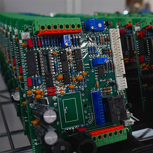
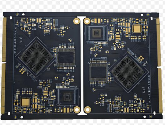
A Multilayer PCB (Printed Circuit Board) is a type of PCB with more than two conductive layers. Unlike a double-sided PCB, which has two copper layers (top and bottom), a multilayer PCB consists of three or more layers of copper, interconnected by copper-plated vias. The number of layers can range from 3 layers to 40 layers or more, depending on the design requirements.
Key Features of Multilayer PCBs:
- Multiple Conductive Layers: At least three conductive layers, typically used for routing, signal transmission, and component mounting.
- Copper Plated Vias: Vias are used to interconnect different layers and provide electrical pathways.
- Layered Design: The design includes top and bottom layers for component placement and internal layers for routing connections.
How to Manufacture a Multilayer PCB?
The manufacturing process of multilayer PCBs is more complex than that of single-sided or double-sided PCBs. It requires careful attention to ensure that the copper layers are properly aligned and interconnected. Here’s an overview of the multilayer PCB manufacturing process:
Steps Involved in Multilayer PCB Manufacturing:
- PCB Layout Design:
- Use PCB design software (e.g., Proteus, Eagle, OrCAD) to create the circuit layout for the multilayer PCB. This design includes top and bottom layers for component placement and multiple inner layers for routing.
- Creating the Inner Layer Core:
- The inner layers are prepared using laminates of the desired thickness, treated with copper foil, dry film resist, and exposed to UV light for pattern transfer.
- Lamination Process:
- The inner layer core is stacked with prepreg boards (a type of insulating material) and additional copper foil sheets. The layers are aligned using alignment holes.
- Applying Heat and Pressure:
- The stacked layers are subjected to heat, pressure, and vacuum using a heated hydraulic press. This ensures that no air remains between the layers, allowing the resin in the prepreg to bond the layers together.
- Curing:
- Once the lamination process is complete, the material is cured, and the prepreg resin binds the layers, forming a solid multilayer PCB.
- Drilling and Via Plating:
- Vias are drilled through the PCB to create interconnections between layers. Copper plating is then applied to the drilled vias.
- Final Etching and Testing:
- The PCB undergoes final etching to remove excess copper and ensure that the copper traces are properly formed. Electrical testing is performed to ensure functionality.
Advantages of Multilayer PCBs
Multilayer PCBs offer several key advantages, especially when it comes to high-density and high-performance designs.
- Reduced Size and Space Saving:
- The ability to have multiple layers means that multilayer PCBs take up less space, making them ideal for compact electronic devices.
- Lightweight:
- With a reduced size and optimized design, multilayer PCBs are typically lighter than alternative circuit boards.
- High Circuit Density:
- Multiple layers provide more space for routing and connecting components, allowing for high-density circuit designs.
- Better Durability and Flexibility:
- Multilayer PCBs are more durable and can handle complex circuits with better reliability.
- Single Connection Point:
- Multiple layers allow for a single connection point for power and ground, making the board more efficient and easier to manage.
Disadvantages of Multilayer PCBs
While multilayer PCBs offer great flexibility and performance, they also come with certain challenges:
- Higher Manufacturing Costs:
- The complex design and manufacturing process makes multilayer PCBs more expensive than single-layer or double-sided boards.
- Complex Design and Production:
- The multilayer design requires advanced tools, skilled designers, and precise manufacturing processes.
- Limited Manufacturers:
- Not all PCB manufacturers have the capability to produce multilayer PCBs, especially with more than 4 layers.
- Highly Skilled Designers:
- Multilayer PCBs require designers with expertise in handling complex layouts, especially for higher-layer counts.
- Increased Production Time:
- The multi-step process required to produce these PCBs leads to longer production times, especially for boards with many layers.
Common Applications of Multilayer PCBs
Due to their high density, compact design, and ability to handle complex circuits, multilayer PCBs are used in a wide variety of advanced applications across several industries. Some common uses include:
1. Computers and Laptops:
- Multilayer PCBs are crucial in computers and laptops, where high circuit density and performance are essential.
2. Telecommunications Equipment:
- Devices such as mobile phones, tablets, and handheld devices rely on multilayer PCBs for compact, high-performance designs.
3. Signal Transmission:
- Cell phone repeaters, GPS systems, and signal transmission equipment use multilayer PCBs to ensure reliable signal routing.
4. Satellites:
- The high reliability and small size of multilayer PCBs make them ideal for satellite electronics.
5. Medical Equipment:
- Multilayer PCBs are used in medical devices such as heart monitors, X-ray machines, and CAT scanners, where precision and reliability are crucial.
6. Industrial Equipment:
- Complex industrial control systems and robotics often require multilayer PCBs to handle high-density circuits.
7. Military and Aerospace:
- Military and aerospace applications, including atomic systems, nuclear equipment, and defense electronics, rely on multilayer PCBs for their performance in harsh environments.
8. Automotive:
- Automotive applications, from engine control units (ECUs) to infotainment systems, often utilize multilayer PCBs for their compact and durable design.
Multilayer PCBs are essential in modern electronics, offering high-density circuit designs, reduced size, and improved durability. While the manufacturing process is more complex and costly compared to single-sided or double-sided PCBs, the performance and capabilities of multilayer PCBs make them indispensable for advanced applications in industries such as computers, telecommunications, medical equipment, and aerospace.
The multilayer PCB design is a critical component in the development of high-performance devices, and as electronic devices continue to become more compact and complex, the demand for multilayer PCBs will only grow.

