Multilayer PCB Manufacturing Process: A Complete Step-by-Step Guide
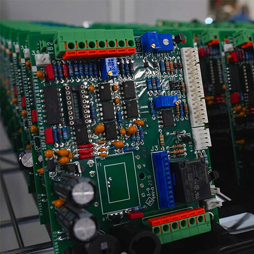
Multilayer printed circuit boards (PCBs) are widely used in modern complex electronics. These PCBs consist of multiple layers of conductive materials stacked on top of each other, enabling the design of more complex circuits with higher functionality. Such complex PCBs are used in various fields such as industrial automation, aerospace, military and medical devices, computers, and smartphones. In this easy-to-understand comprehensive guide, we will walk you through each stage of the multilayer PCB manufacturing process — from design layout to etching, lamination, and final testing.
What is a Multilayer PCB?
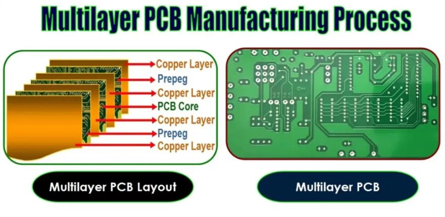
A multilayer PCB is a printed circuit board that consists of more than two layers, typically at least three or more layers of conductive copper, separated by an insulating material (substrate). These layers are stacked and connected by vias, resulting in a compact and efficient PCB design.
Multilayer PCB Manufacturing Steps and Flowchart
| Step # | Process Description |
|---|---|
| 1. Design and Layout | Create the PCB layout using CAD software. |
| 2. Material Selection | Select the substrate (e.g., FR4), prepreg, and copper layer. |
| 3. Inner Layer Imaging | Apply photoresist and transfer the circuit pattern using UV light. |
| 4. Etching | Remove unwanted copper using chemicals. |
| 5. Lamination | Stack and bond copper layers with insulating prepreg under heat and pressure. |
| 6. Drilling | Drill holes to connect different layers. |
| 7. Plating | Electroplate the drilled holes to create conductive paths between layers. |
| 8. External Layer Imaging | Repeat imaging and etching of external layer copper. |
| 9. Applying Solder Mask | Apply protective solder mask to prevent shorts and corrosion. |
| 10. Silkscreen | Print component labels and other details for easy identification. |
| 11. Surface Treatment | Apply protective surface treatment to exposed copper pads. |
| 12. Electrical Testing | Test for opens, shorts, and other electrical faults. |
| 13. Quality Inspection | Perform visual and automated inspections to detect defects and ensure accuracy. |
Steps Involved in Multilayer PCB Manufacturing Process
Step 1. Design and Layout
The first step is to create the PCB layout using computer-aided design (CAD) software. Engineers design the circuits and layer arrangements, ensuring accurate connections between electronic components and layers. PCB design tools such as Altium Designer or KiCAD are often used for this task.
Step 2. Material Selection
It is important to choose the correct PCB substrate and core materials, prepreg (insulating material), and copper layers. The substrate is usually FR4 (glass-reinforced epoxy laminate), which provides structural stability and insulation, while the copper sheets serve as conductive layers.
Step 3. Inner Layer Imaging
The PCB manufacturing process begins with the creation of the inner layers. A photosensitive material, called photoresist, is applied to the copper layer. UV light is then used to transfer the desired circuit pattern, leaving areas where the copper needs to be etched away.
Step 4. Etching
After imaging, chemicals like ferric chloride or ammonium persulfate are used to etch away the exposed copper. This process removes unwanted copper, leaving the desired circuit traces. The photoresist is then stripped off, revealing the final copper pattern of the inner layers.
Step 5. Lamination
Lamination is the process of bonding multiple layers of copper and insulating material (prepreg) together. The inner layers are stacked on top of each other, with the outer layers on the top and bottom. The stack is placed in a high-pressure, high-temperature press to bond the layers into a single PCB.
Step 6. Drilling
In this step, precision holes (called vias) are drilled into the PCB to connect different layers. A high-speed drill equipped with a tungsten carbide drill bit ensures precision and accuracy.
Step 7. Plating
After drilling, the holes are plated with copper to create electrical connections between layers. This is done through a chemical process that deposits a thin layer of copper on the walls of the drilled holes, ensuring conductivity between the layers.
Step 8. Imaging and Etching of External Layers
Similar to the inner layers, the external layers are imaged and etched to create the circuit pattern. A layer of photoresist is applied to the outermost copper, and then the design is transferred using UV light. The unwanted copper is then etched away, and the photoresist is removed.
Step 9. Solder Mask Application
The surface of the PCB is coated with a protective solder mask. This layer insulates the board and protects the copper traces from corrosion or damage. Only the areas where components will be soldered are exposed.
Step 10. Silkscreen
Silkscreen is printed on the surface of the PCB to display important information such as component labels, logos, or serial numbers. This step ensures easier PCB assembly and component identification.
Step 11. Surface Treatment
Surface treatment is applied to protect the exposed copper pads and ensure good solderability during component assembly. Common surface treatments include HASL (hot air solder leveling), ENIG (electroless nickel immersion gold), and OSP (organic solderability preservative).
Step 12. Electrical Testing
Before the PCB is shipped, electrical testing is performed to check for any opens, shorts, or defects. This ensures that the PCB functions as designed and that there are no manufacturing errors.
Step 13. Quality Inspection
A thorough visual inspection using automated optical inspection (AOI) systems ensures that the PCB meets quality standards. The inspection includes checking for proper layer alignment, hole positioning, and good surface finish.
Multilayer PCB manufacturing is a complex and highly precise process that requires expertise, experience, and careful attention to detail at every step. By following the above process, manufacturers can produce high-quality multilayer PCBs for advanced and complex electronic products.

