Multilayer PCB Design Essentials
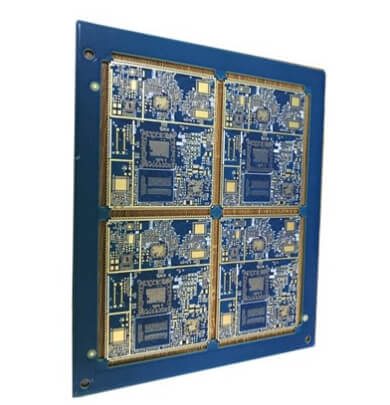
Multilayer PCB design follows principles similar to double-layer design, with added structural complexity and a focus on stable signal integrity and efficient routing. With experience in double-layer PCBs, moving to multilayer designs can be manageable.
1. Define the Layer Stack-Up
- Symmetry and Centering: Design the stack symmetrically around a central substrate layer for balance, and use ground planes to separate signal layers.
- Layer Types and Structure: Common configurations include 4-layer, 6-layer, 8-layer, or even 16-layer setups. In general:
- Top and bottom layers are typically designed using microstrip line models.
- Internal signal layers are best analyzed with stripline models.
- For high-layer-count boards (10+ layers), simulate signal behavior via software to ensure optimal routing and isolation.
2. Ground Layer Isolation and Routing Practices
- Isolation: Use ground layers to isolate adjacent signal layers, minimizing cross-talk and interference.
- Routing and AC Loop Avoidance: In designs with multiple layers (e.g., 6, 10, or more), ensure perpendicular routing on adjacent layers to prevent AC loops. Avoid segmenting the ground layer, and prioritize placing thick power lines on the signal layers where additional power supplies are needed.
3. Manufacturer Specifications for Impedance Matching
- Obtain Key Parameters: Request dielectric constant, line width, copper thickness, and board thickness from the PCB manufacturer, as they’ll inform impedance matching.
- Calculate Dimensions: Based on the provided parameters, determine line width, line spacing (using the 3W rule for separation), and line length for precision in high-speed applications.

4. Blind, Buried, and Through-Hole Options
- Vias and Layer Types: Choose between blind vias, buried vias, and traditional through-holes, based on board thickness and complexity. Be mindful that while these options enhance wiring capabilities, they increase production cost.
- PCB Thickness Constraints: For boards that must fit into tight slots (like PCI), consider custom stack configurations, such as using fewer layers on the edges while maintaining higher layer counts in the center.
5. Inner vs. Outer Layer Routing for Stability
- High-Speed Signals: Route high-speed lines on inner layers to shield them from environmental factors (temperature, humidity) affecting outer layers.
- Testing Considerations: For any necessary testing, add test vias to expose signals without disrupting the internal layers, avoiding direct flying wires or rework on high-density, high-frequency multilayer boards.
6. Planning and Precision
- Meticulous Design: High-density, multilayer boards leave little room for error. Design carefully on paper and ensure calculations are correct to avoid costly rework.
- Single Pass Success: Due to the complex, layered nature of these boards, aim for accuracy from the start. Incomplete or inaccurate layouts may require board redesign, impacting budget and timelines.
KKPCB conducts research on special processing technologies such as ordinary double-sided boards, thick copper circuit boards, high-frequency circuit boards, HDI circuit boards, rigid-flexible circuit boards, FPC flexible boards, buried blind hole circuit boards, and IC carrier boards. Provides PCB design, PCB layout, PCB prototyping and PCB assembly services.


