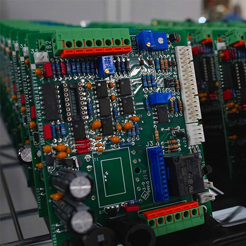
How Multilayer PCB Assembly is Made, Advantages and Applications
Printed Circuit Boards (PCBs) are valuable electronic components that help improve the efficiency and performance of machines. Therefore, regardless of size, number of production units and purpose, vigilance must be maintained in their manufacturing process. However, what needs to be considered is the use of different types of PCBs. Multilayer PCBs account for more than 50% of the circuit board market as it has multiple layers that ensure higher productivity. Moreover, multilayer PCBs are in high demand due to smaller, faster and more powerful devices. Usually, copper is used as a conductor, which ultimately increases the current carrying capacity.
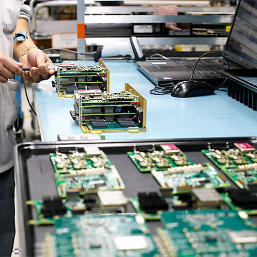
PCBs with more than 2 conductive layers are called multilayer PCB assemblies. From the appearance, they look like a combination of double-sided circuit boards with laminates bonded with thermal insulation layers in between. These combinations are made in a proper arrangement so that both layers are exposed to the environment for better connections. Once the board is ready, through-holes such as blind and buried vias and plated through-holes are used to establish connections between layers.
The emergence of multilayer PCB assembly is a result of the needs of advanced electronics. In the past few years, electronic devices have been working more aggressively and advanced. They demand better and more complex PCBs to make compromises in performance. However, PCBs always face difficulties in designing. Many manufacturers have reported problems such as crosstalk, noise, and stray capacitance, which directly affect the performance level – whether it is a single-sided or double-sided PCB. This is when the concept of multilayer PCB assembly comes into being.
Process
There is no hard and fast rule for manufacturing multi-layer PCBs. The process is very simple as it includes the following steps:
Material selection of prepreg board, copper foil, and inner core.
Prepreg board is made using glass cloth and epoxy resin.
The copper foil covered on the core board has a specific thickness and weight.
The core board laminate is covered with a photosensitive dry film, which uses ultraviolet light to irradiate the photoresist, which receives the electronic data from the internal circuit and starts working.
This is a single core lamination process that is not applicable to multilayer PCB assembly. It has a completely different method, as described below:
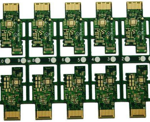
Multilayer lamination process
Usually, this is a continuous lamination process consisting of a copper foil base layer and a prepreg layer. The only thing to consider is the number of prepreg layers, which vary depending on the requirements of the operation. Subsequently, the inner core takes its place on the layer and is then covered with a copper foil layer for the second time. The result is called a multilayer PCB stack. Many laminates are stacked up in the same manner. When completed, the final laminate stack is called a “book” and the laminates are called “chapter”.
Once completed, the board is fed into a hydraulic press to apply pressure and create a vacuum as part of the curing. This step is responsible for pressing the laminate and letting the prepreg resin fuse with the foil and core. After that, the resultant is taken out and placed in a cooler place to bring its temperature down to normal levels so that the resin can settle. This is how multilayer copper PCBs are manufactured.
Advantages
From increasing productivity to driving the advancement of electronic products, multilayer PCB assemblies have the following advantages:
Compact size: The presence of multiple layers is the main feature that makes this type of PCB smaller in size compared to other PCBs. As electronic PCB manufacturers are trying to make space-saving machines, multilayer PCBs occupy a smaller area than before, thus playing an important role in their internal circuits. Whether it is a smartphone, tablet, laptop or wearable device, they can easily fit into any space.
Lightweight body: Smaller size and lighter weight, especially when using single or double-layer PCBs to connect multiple connectors respectively.
High quality: By investing a lot of time and effort in manufacturing multi-layer PCB assemblies, customers can expect better quality than double and single-layer PCBs.
Better durability: In addition to the previous point, multi-layer PCBs must also guarantee durability and reliability to withstand their own weight as well as the heat and pressure generated when bonding. The insulation layer between the circuits as well as the protective material and pre-impregnated adhesive ensure that it is more satisfactory in any situation.
More powerful function: Multi-layer PCBs are high-density components that can be used as close connections of circuit boards to establish stronger connections. Its electrical characteristics help achieve higher speeds and greater capacity in smaller sizes.
Disadvantages
There are some disadvantages in using multi-layer PCB assemblies, especially for complex and cheap electronic products.
Higher cost: Multi-layer PCB assemblies have better performance, but the price is slightly higher compared to double and single-layer PCBs. Its manufacturing process is cumbersome, the design is complex, and requires a lot of attention, making it expensive for some customers. Moreover, any problem or omission in the manufacturing process can lead to huge losses as rework will be more complicated, resulting in more money and labor expenditure.
Complex Production: These PCBs require more effort and time to design and manufacture. Even a small flaw can ruin all the efforts.
Limited Supply: Multilayer PCBs require a specific type of machine to manufacture. They are very expensive and not every producer can afford them or even have the labor to operate them. Ultimately, this limits the production of multilayer PCB assembly for customers.
Need for Professional Designers: As mentioned above, multilayer printed circuit boards are completely different from other PCBs, and they require professional designers to smoothly carry out extensive designs. Make sure that the designer is experienced and well aware of the techniques to make connections between layers and solve impedance and crosstalk issues at the same time.
Production Time: The complexity and requirements of manufacturing are directly proportional. The more complex the connections, the higher the manufacturing requirements. Therefore, the turnover rate of multilayer PCB assembly is low due to long production time and labor-intensive work.
How Multilayer PCB Assembly is Made, Advantages, and Applications
After knowing the advantages, disadvantages, and comparison with other PCBs, one question is sure to arise in everyone’s mind: Why and where are these multilayer PCBs used? Here are the answers:
Consumer Electronics: This category covers a wide variety of products that make the most of multilayer PCB assemblies in various ways. While other types of PCBs are also designed for this purpose, there is one thing that makes multilayer PCBs more advantageous – that is consumer trends. Today, electronic manufacturers prefer these PCBs for their ability to be easily integrated into multifunctional smart devices and gadgets. From smart watches to universal remote controls, multilayer circuit boards have come a long way.
Computer Equipment: Whether it is a motherboard or any server, these PCBs are very useful due to their high functionality and space-saving features.
Telecommunications: Telecommunication experts can use the services of multilayer PCB assemblies in several fields, whether it is satellite applications, signal transmission, or GPS. Their functionality and durability allow them to be used even in outdoor towers or mobile devices.
Industrial: There is no doubt that these PCBs can provide better durability compared to other options. First of all, they are suitable for daily rough handling. Moreover, industrial controls also make the most of multilayer PCB assemblies. Whether it is control systems or industrial computers, they can be used in industrial and manufacturing applications.
Medical Equipment: Apart from industrial and telecommunications, medical is another industry that makes the most of the features of PCBs. Today, many diagnostic and therapeutic machines are equipped with multi-layer PCB assemblies – thanks to their light weight, powerful features, and compact size. Heart monitors, medical testing equipment, X-ray equipment, and CAT scan equipment make the most of PCBs.
Defense and Military: Due to the reasons and features mentioned above, these high-speed circuits are able to enhance defense equipment. They are able to support highly compact engineering designs with small size and excellent construction.
Automobile: The modern era has incorporated electronic components into vehicles. Whether it is GPS, engine sensors, or headlight switches, everything is operated by these electronic components, which are supported by multi-layer PCB assemblies. In addition to durability, these PCBs have also proven to be heat-resistant and highly functional in automobiles.
There are many more aspects that can be discussed about the role of multi-layer circuit boards. All that customers need to consider before deciding to place an order with a manufacturer is the quality and features of the printed circuit boards.
KKPCB conducts research on special processing technologies such as ordinary double-sided boards, thick copper circuit boards, high-frequency circuit boards, HDI circuit boards, rigid-flexible circuit boards, FPC flexible boards, buried blind hole circuit boards, and IC carrier boards. Provides PCB design, PCB layout, PCB prototyping and PCB assembly services.

