


Microvia Reliability in High-Density Designs
As high-density interconnect (HDI) designs with larger layer counts become more prevalent, the use of microvias is increasing. In builds with 3+N+3 or larger configurations, sequential lamination now often relies on skipped vias, staggered microvias, and stacked microvias. However, one of the key challenges is that microvias are more susceptible to failure than plated through-holes. The small size and incomplete depth of microvias make them more susceptible to stress, which increases the likelihood of failure during reflow, accelerated testing, or actual operating conditions. Read on as we discuss the causes and solutions to microvia reliability issues.
The transition from tin-lead solder to high-tin alloys has resulted in an increase in operating temperatures.
These higher temperatures pose risks to copper interconnects and substrates during the reflow process.
Microvias are susceptible to damage during PCB assembly due to exposure to high temperatures.
Mismatched Expansion Rates
During the reflow process, glass epoxy expands by 200 parts per million (ppm), while copper expands by 16 ppm.
Significant differences in expansion rates can cause stress and potentially cause microvia connections to fail.
Multiple Lamination Cycles
HDI (High Density Interconnect) boards may require multiple lamination cycles.
Prolonged exposure to high temperatures and pressures during these cycles can affect the durability of plated vias.
Reflow Stress
The resistance of a microvia should not increase by more than 5% during a reflow cycle.
Increased resistance is a sign of potential failure.
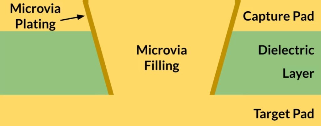
Microvia failures typically occur at the interface of the capture pad and the target pad (see figure below)
Buried Vias
Microvias on buried vias are more susceptible to failure, especially when the via barrel length is long.
This is due to additional thermal stress and expansion issues that affect reliability.
Thermal Limits of Materials
Material degradation is a key factor in failure, especially at temperatures above the glass transition temperature (Tg) of FR4.
Increased thermal expansion at high temperatures can create mechanical stress that can damage microvias.
Preconditioning and Resistance Changes
The resistance in the microvias changed significantly during preconditioning at 245°C and 260°C.
These resistance changes stabilize after preconditioning, but material or structural damage may still be present.
Microvia Diagram.
Microvia Reliability Standards
IPC has developed rigorous microvia reliability test methods, outlined in IPC-TM-650, see Methods 2.6.27 and 2.6.7.2.
Method 2.6.27 involves subjecting the test vehicle or coupon to a standard solder paste reflow profile with a peak temperature of 230°C or 260°C. The coupon is connected to a 4-wire resistance measurement device to monitor for resistance increase, which must remain below 5% during six complete reflow cycles. The daisy chain in the test coupon consists of functions used in the actual circuit to simulate real-world conditions.
Method 2.6.7.2 introduces a thermal shock test, where the test coupon is subjected to 100 thermal shocks between -55°C and 210°C. Resistance is monitored once per second during reflow and once per cycle during the thermal shock test. If the resistance increases by more than 5%, the device is considered to have failed.
Design Guidelines for Reliable Microvias
Choose Dielectric Materials Compatible with Laser Drilling
Laser drilling creates precise V-shaped holes, making the plating process smoother and more efficient. To prevent uneven heating and material inconsistencies, choose dielectric materials that are compatible with laser drilling. Some recommended materials include:
Isola FR408HR: A high-performance, low-loss dielectric material known for its excellent thermal and mechanical properties, ideal for high-speed digital and RF applications.
Isola FR370HR: Designed for high-temperature reliability, this material is suitable for multi-layer PCB designs that require thermal performance and durability.
I-speed: A high-speed, low-loss laminate with stable dielectric properties that provides better signal integrity and lower transmission losses, especially in high-frequency applications.
Nelco N7000-2HT: A high-temperature, low-loss dielectric material that excels in high-speed and high-frequency applications, providing excellent electrical and thermal performance for complex PCB designs.
Follow IPC-T-50M Microvia Standards
The IPC-T-50M standard provides basic guidelines for microvia design to ensure reliability. Key parameters include:
Maximum aspect ratio of 1:1
Maximum diameter of 6 mm
Maximum distance between capture pad and target pad of 10 mil
Prefer staggered microvias over stacked microvias
Staggered microvias are more resistant to thermal cycling than stacked microvias. When designing staggered microvias, ensure that the vertical spacing between them is greater than the hole diameter. This spacing helps reduce stress and improve reliability during thermal cycling.
Follow IPC-2226 Stackup Standards
Choosing a PCB stackup configuration that complies with the IPC-2226 standard is critical for manufacturability and cost-effective production. Here are the various IPC-2226 stackup types that support microvia reliability:
Type I: One PTH and one microvia layer on one or both sides of the core.
Type II: PTH, buried vias, and a single microvia layer on one or both sides of the core.
Type III: Includes PTHs, buried vias, and at least two microvia layers on one or both sides of the core.
Staggered Type III: Has staggered microvias with at least two microvia layers on one side of the core.
Capped and Staggered Type III: Has staggered microvias and capped outer layers and two PTHs, one of which is capped.
Ensure Zero Clearance Between Solder Mask and Microvias
To prevent solder bridging during reflow, any gaps between solder mask and microvias must be eliminated. Solder can flow into these gaps, causing unintended connections between adjacent traces, a serious design flaw that must be avoided.
Use Simulation Tools for Microvia Reliability
Simulation tools, such as Gauss Stack’s Microvia Reliability Simulation, allow designers to predict and mitigate potential issues before building expensive test boards. This fast simulation environment allows you to model a variety of scenarios, helping to optimize design choices and avoid time-consuming trial and error.
Optimize Microvia Size and Spacing
The size and spacing of microvias are critical to the overall reliability of the PCB. Larger microvia diameters, especially 6 mils or larger, provide greater resistance to thermal stress. Similarly, increasing the pitch (the distance between microvias) to at least 10 mils minimizes the risk of failures due to copper cracking or substrate debonding during thermal expansion.
Balancing Microvia Density and Reliability
While larger microvias and wider pitches can improve reliability, they also reduce available board space. Designers must carefully balance microvia size and pitch with the need for tight routing, especially in high-density applications where reliability is critical, such as aerospace and military electronics.
Use microvias with a diameter of 6 mils or larger.
Keep aspect ratios below 0.75:1, preferably 0.64:1 or less for best reliability.
Ensure a minimum spacing of 10 mm between microvias.
Additionally, staggered microvia arrangements are preferred over stacked microvias, especially in designs that experience significant thermal cycling. Staggered configurations improve reliability and yield, even in challenging environments.
Consider Thermal Stress During Reflow
The reflow process is particularly demanding on microvias, subjecting them to extremely high heat. Larger microvias with lower aspect ratios are better able to withstand the thermal cycles during the reflow process. For designs that require lead-free soldering (higher reflow temperatures) or that require multiple reflows, larger microvias and wider spacing are recommended to relieve thermal stress.
Methods of Microvia Failure
Microvia failure modes include a variety of defects that arise from material and process variations. Here is a brief overview of common microvia failure modes:
Microvia separation from target pad: This separation is typically caused by thermal stress and physical strain. It typically starts from the dielectric foot at the bottom of the microvia. This separation can lead to failure during the cooling cycle and may produce cracks.
Barrel cracks can occur within the cylindrical portion of the microvia, typically during the heating phase of the thermal cycle. These cracks are associated with thin copper plating, and plating issues can exacerbate the cracks and cause the microvia to crack.
Corner cracks: These cracks form at the interface between the positioning pad and the target pad due to z-axis expansion. While relatively uncommon, they represent wear-out-type failures that can be caused by other design or material defects.
Circumferential cracks develop around the base of a microvia within a capture pad due to mechanical and thermal stresses, challenging the integrity of the microvia.
Microvia misalignment: This involves the microvia being misaligned from its intended location on the pad, resulting in potential electrical failures such as opens or shorts.
Target pad pullout: Occurs primarily in flex circuits with high CTE and low Tg materials such as acrylic adhesives, resulting in vertical and circumferential cracking around the target pad.
Copper voids: These voids in the copper fill of a microvia can compromise structural integrity, especially when the voids are large enough to affect the wall thickness of the microvia barrel.
Copper cap separation: In stacked microvias, copper cap separation due to different expansion rates with the dielectric can disrupt the conductive path and cause failure.
How OrCAD X Enables More Reliable Microvias
OrCAD X Features
HDI Routing with Microvias
OrCAD X provides advanced HDI (High Density Interconnect) routing tools that allow users to easily add blind, buried and microvias. The constraint manager automatically selects the correct vias based on the design rules.
Proper selection and placement of microvias is critical to reduce stress on the microvias during reflow and thermal cycling and improve reliability.
OrCAD X enables designers to define rules for stacking, staggering or skipping microvias in the constraint manager, ensuring that the microvia arrangement meets reliability standards.
Staggered microvias are better suited for achieving better thermal cycling reliability as they reduce inter-layer stress and improve overall durability.
Real-time Constraint-Driven DRC Checking
The OrCAD X constraint manager provides real-time feedback on spacing, via placement and material usage, alerting designers to any potential violations.
Instant feedback during the design process helps prevent violations that could lead to increased mechanical or thermal stress on the microvias.
Cross-Section Editor for Stack-Up Design
OrCAD X allows for detailed layer and material configuration using the Cross-Section Editor, including dielectric properties and material thickness, which is critical for controlling thermal expansion.
Proper layer and material configuration ensures that thermal expansion rates between materials are well managed, preventing stress-induced failures.
Thermal Simulation Tools
Thermal analysis tools used in conjunction with OrCAD X help simulate heat distribution across the board, identifying areas of potential thermal stress on microvias.
Manufacturing defects can significantly reduce the life of microvias, and DFM checks help ensure that the design is ready for reliable production.
Constraint Management for HDI Designs
OrCAD X supports detailed constraint management for HDI designs, including specific rules for defining microvia diameter, spacing, and aspect ratio.
Ensuring correct microvia size and location is critical to preventing failures associated with high current density and thermal cycling.
DFM (Design for Manufacturability) Checks
OrCAD X includes DFM checks to ensure that microvias meet manufacturing tolerances and reliability standards, helping to avoid defects during production.
Manufacturing defects can significantly reduce the life of microvias, and DFM checks help ensure that the design is ready for reliable production.
To ensure microvia reliability in PCB design, engineers should focus on challenges such as thermal stress, material expansion, and copper integrity. Cadence OrCAD X provides advanced features such as HDI routing, real-time DRC checking, and thermal simulation, allowing designers to optimize microvia placement for improved durability. Optimize articles and meet Google SEO optimization, layout keywords,
Microvia Reliability in High-Density Designs: Causes, Solutions, and Design Guidelines
The use of microvias has become more common as the number of layers in high-density interconnect (HDI) designs increases. In the build of 3+N+3 or larger configurations, sequential lamination often relies on skipping vias, staggered microvias, and stacked microvias. However, microvias are more prone to failure than plated through holes, mainly due to their smaller size and incomplete depth, making them more susceptible to stress. This article will delve into the causes, solutions, and design guidelines of microvia reliability issues to help engineers optimize high-density PCB designs.high-density PCB designs.
Causes of Microvia Reliability Issues
Factor Details
High-Temperature Dielectric Materials The transition from tin-lead solder to high-tin alloys results in higher operating temperatures, increasing the risk of microvia damage during reflow.
Expansion Rate Mismatch The significant difference in expansion rate between glass epoxy (200 ppm) and copper (16 ppm) leads to stress concentrations that can cause microvia connection failures.
Multiple Lamination Cycles HDI boards require multiple lamination cycles, and prolonged exposure to high temperatures and stresses can affect the durability of plated vias.
Reflow Stress The microvia resistance should not increase by more than 5% during reflow cycles, otherwise it may indicate a potential failure.
Buried Via Issues Microvias on buried vias are more susceptible to failure due to thermal stress and expansion issues, especially when the via barrel is long.
Thermal Limits of Materials Material degradation and increased thermal expansion at temperatures above the glass transition temperature (Tg) of FR4 can damage microvias.
Preconditioning and Resistance Changes The microvia resistance changes significantly during preconditioning at 245°C and 260°C, which may cause material or structural damage.
Microvia Reliability Standards
IPC has developed a strict microvia reliability test method, mainly based on methods 2.6.27 and 2.6.7.2 in IPC-TM-650:
Method 2.6.27: The test vehicle or sample undergoes 6 cycles in the reflow curve at 230°C or 260°C, and the resistance increase shall not exceed 5%.
Method 2.6.7.2: The sample undergoes 100 thermal shocks between -55°C and 210°C, and the resistance increase exceeds 5% is considered a failure.
Design Guidelines for Reliable Microvias
- Select dielectric materials compatible with laser drilling
Recommended materials include:
Isola FR408HR: high performance, low loss, suitable for high-speed digital and RF applications.
Isola FR370HR: high temperature reliability design, suitable for multi-layer PCBs.
I-speed: high speed, low loss, providing better signal integrity.
Nelco N7000-2HT: high temperature, low loss, suitable for high-frequency applications.
- Follow IPC-T-50M microvia standard
Maximum aspect ratio: 1:1
Maximum diameter: 6 mm
Maximum distance between capture pad and target pad: 10 mil
- Use staggered microvias first
Staggered microvias are more resistant to thermal cycling than stacked microvias, and it is recommended that the vertical spacing is greater than the hole diameter. - Follow IPC -2226 Stacking Standards
- Choose the appropriate stacking type (e.g., Type I, II, III) to ensure manufacturability and reliability.
- Eliminate gaps between solder mask and microvias
Prevent solder bridging and avoid accidental connections between adjacent traces. - Use simulation tools to optimize the design
Such as Gauss Stack’s microvia reliability simulation, help predict and mitigate potential issues. - Optimize microvia size and spacing
Microvia diameter is recommended to be 6 mils or larger. - Aspect ratio is kept below 0.75:1, with an optimal value of 0.64:1.
- Microvia spacing is at least 10 mils.
- Balance microvia density with reliability
In high-density applications, microvia size and spacing need to be weighed against routing requirements. - Consider thermal stress during reflow
For lead-free soldering or multiple reflow designs, larger microvias and wider spacing are recommended. - Microvia Failure Modes
- Microvia separation from target pad: Caused by thermal stress and physical strain, usually starting from the dielectric foot at the bottom of the microvia.
- Barrel crack: Occurs in the cylindrical portion of the microvia and is associated with thin copper plating.
- Corner crack: Formed at the interface of the capture pad and target pad, caused by z-axis expansion.
- Circumferential crack: Caused by mechanical and thermal stresses, affecting microvia integrity.
- Microvia misalignment: Causes electrical failures such as opens or shorts.
- Target pad pull-out: Common in flex circuits, causes cracking around the target pad.
- Copper voiding: Compromises the structural integrity of the microvia.
- Copper cap separation: In stacked microvias, different expansion rates lead to the destruction of the conductive path.
- How OrCAD X enables more reliable microvias
- Feature Description
- HDI routing support Provides automatic selection and placement of blind, buried and microvias to reduce stress.
- Live DRC Checking Provides real-time feedback on spacing, via placement, and material usage to prevent violations.
- Cross-Section Editor for Stacked Design Supports detailed layer and material configuration to optimize thermal expansion management.
- Thermal Simulation Tool Simulates board heat distribution to identify potential thermal stress areas.
- DFM Checking Ensures microvias meet manufacturing tolerances and reliability standards to avoid production defects.
- To ensure microvia reliability in PCB design, engineers need to focus on challenges such as thermal stress, material expansion, and copper integrity. By selecting the right materials, following design standards, optimizing microvia size and spacing, and combining simulation tools such as OrCAD X, microvia durability and overall design reliability can be effectively improved.