LTCC Multilayer Substrates
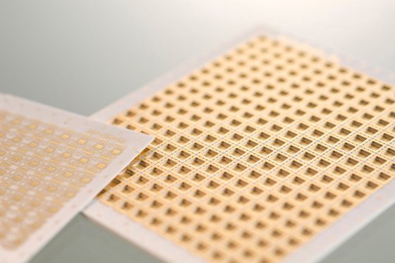
KKPCB LTCC substrates with silver conductor material provide multilayer substrates with low dielectric loss. Coils, capacitors and resistors can be embedded in the inner layer. Ideal for high-frequency modules and silicon wafer interposer substrates.
Features
KKPCB LTCC substrates can embed coils, capacitors and resistors, thereby reducing the substrate size. Excellent dimensional tolerance of ±0.3% improves mounting accuracy. Low conductor loss is achieved by using Ag conductor material. Electroless Ni/Au or Electroless Ni/Pd/Au can be selected for surface treatment.
Material Characteristics
| ITEM | UNIT | TEST CONDITIONS | NL-Ag3 |
|---|---|---|---|
| COLOR | ― | ― | WHITE |
| DENSITY | g/cm3 | ― | 2.85 |
| BENDING STRENGTH | MPa | ― | 250 |
| THERMAL EXPANSION | 10-6/℃ | RT~350℃ | 5.5 |
| THERMAL CONDUCTIVIT | W/(m・K) | ― | 3.5 |
| DIELECTRIC | ― | 2.3GHz | 7.1 |
| LOSS TANGENT | % | 2.3GHz | 0.3 |
Values are typical values
Design Guidelines
| ITEM | UNIT | STANDARD | CUSTOM | |
|---|---|---|---|---|
| DIMENSIONS | inch | 2~4 | ー | |
| TOLERANCE | % | ±0.35 | ー | |
| THICKNESS TOLERANCE | % | ±10 | ー | |
| # OF LAYERS | Layer | 2~ | ー | |
| VIA DIAMETER | mm | 0.15, 0.2 | 0.1 | 0.085 |
| VIA PAD DIAMETER | mm | VIA DIAMETER +0.15 | VIA DIAMETER +0.1 | VIA DIAMETER +0.05 |
| VIA PICTH | mm | 0.5 | 0.35 | 0.25 |
| LINE/SPACE | mm | 0.1/0.1, 0.15/0.15 | 0.075/0.075 | |
| LINE/VIA PAD DISTANCE | mm | 0.2 | 0.1 | |
| VIA EDGE/SUBSTRATE EDGE DISTANCE | mm | 0.5 | 0.25 | |
| LINE/SUBSTRATE EDGE DISTANCE | mm | 0.3 | 0.15 | |
| CAVITY WALL WIDTH | mm | ≧0.5 | 0.35 | |
| CAVITY DEPTH | mm | LESS THAN 2/3 OF TOTAL THICKNESS | ー | |
| CAVITY CORNER R | mm | 0.15, 0.2 | 0.1 | |
| CAVITY BOTTOM THICKNESS | mm | ≧0.3 | ー | |
Product application scenarios
- High-Frequency application substrates (Front-end modules, Sensor substrates)
- Substrates for small package devices
- Silicon wafer interposer substrates
Free consultation with easy form that only takes 90 seconds
Feel free to contact us to ask about our products and services.


