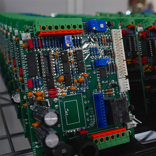
Laminate: HF-140
HF-140 is a high-frequency laminate designed for RF, microwave, and high-speed digital applications. Its unique properties ensure low signal loss, stable electrical performance, and compatibility with complex circuit designs, making it suitable for demanding environments such as telecommunications, aerospace, and automotive systems.
Key Features
- Low Loss Performance
- Minimal dielectric and conduction losses for superior signal integrity.
- Stable Dielectric Constant (Dk)
- Consistent Dk over a broad frequency range enhances design accuracy.
- Low Moisture Absorption
- Maintains electrical and mechanical properties in high-humidity environments.
- Thermal Reliability
- High glass transition temperature (Tg) and low coefficient of thermal expansion (CTE).
- Process Compatibility
- Easily integrates with standard PCB fabrication processes.
Technical Specifications
| Property | Value |
|---|---|
| Dielectric Constant (Dk) | ~3.5 (10 GHz) |
| Dissipation Factor (Df) | ≤ 0.003 (10 GHz) |
| Thermal Conductivity | ~0.5 W/m·K |
| Moisture Absorption | < 0.05% |
| CTE (X-Y) | ~13 ppm/°C |
| CTE (Z) | ~30 ppm/°C |
| Flammability Rating | UL 94 V-0 |
| Peel Strength (1 oz Copper) | ≥ 8 lbs/in |
| Operating Temperature Range | -40°C to +150°C |
Applications
- RF and microwave communication systems
- Satellite and aerospace systems
- Automotive radar systems
- 5G infrastructure
- High-speed digital and mixed-signal circuits
Processing Guidelines
Storage and Handling
- Store flat in a clean, dry environment with controlled humidity.
- Avoid mechanical stress or contamination.
Drilling and Routing
- Use carbide or diamond-coated tools.
- Implement appropriate entry/exit materials to minimize burrs.
Lamination
- Precondition by baking at 120°C–150°C to remove moisture.
- Use compatible prepregs for multilayer designs.
Plating and Etching
- Standard PCB copper plating and etching processes are supported.
- Ensure thorough surface cleaning for optimal adhesion.
Assembly
- Compatible with lead-free and traditional soldering methods.
Advantages
- High signal integrity for high-frequency applications
- Durable and reliable in extreme environments
- Easy processing with standard fabrication techniques

