


KKPCB Case Study: Hybrid Power+RF PCB for Base Station Applications
1. Customer Profile
Client: Anonymous
Industry: Telecom Infrastructure, 5G Macro/Micro Base Stations
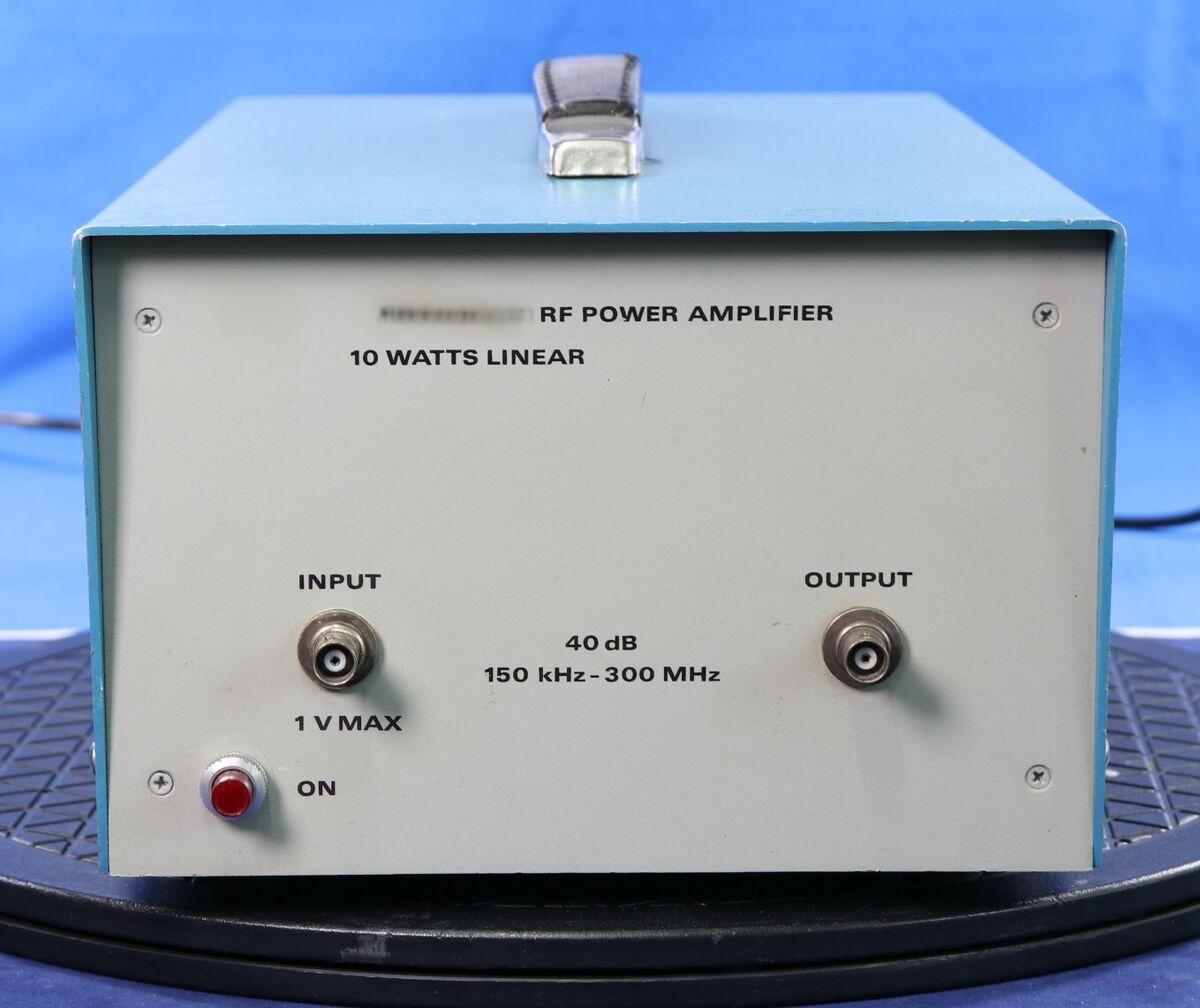
Application: Power Amplifier (PA) Modules + RF Front-End PCBs
High-power base station equipment requiring PCBs are able to handle:
- High current (30A+) for PAs
- Low-loss RF (3.5GHz-28GHz for 5G)
- Thermal stability (85°C ambient, 125°C local hotspots)
Key Challenges Faced:
- Delamination risk from mixed thick-copper (6oz) and RF layers.
- EMI coupling between power and RF sections.
- Thermal warping under high thermal cycling.

2. KKPCB’s Hybrid Power+RF PCB Solution
(A) Material Selection & Stackup
| Layer | Material | Function | Key Specs |
|---|---|---|---|
| L1-2 | Rogers RO4350B | RF Signal (28GHz mmWave) | Dk=3.66, Df=0.0037 @ 10GHz |
| L3-4 | IT-180A (6oz Cu) | High-Current DC Power | 175µm Cu, 10A/mm² current density |
| L5-6 | Isola FR408HR | Digital Control / Mixed Signal | Tg=180°C for thermal stability |
Hybrid Bonding:
- Plated slots for low-inductance power-ground connections.
- Buried copper coin heatsinks under GaN transistors.
(B) Critical Design Features
✅ Ultra-Low RF Loss: 0.4dB/inch @ 28GHz (vs. 1.2dB in standard FR4).
✅ Power Integrity: <5mV ripple under 30A dynamic load.
✅ Thermal Management: 3W/mK thermal vias under PAs (reduce hotspot ΔT by 25%).
✅ EMI Shielding: Copper-filled via fences between RF and power sections.
3. Performance Results vs. Competitors
| Parameter | Old PCB | KKPCB’s Solution | Improvement |
|---|---|---|---|
| Insertion Loss (28GHz) | 1.1dB/inch | 0.4dB/inch | 64% ↓ |
| Max Current (Continuous) | 20A | 35A | 75% ↑ |
| Thermal Resistance (PA Zone) | 12°C/W | 7°C/W | 42% ↓ |
| Production Yield | 82% | 98% | 16% ↑ |
Field Test (5G Base Station):
- 40% Longer MTBF (Mean Time Between Failures) vs. previous supplier.
- Passed MIL-STD-810G vibration/shock tests for outdoor deployments.
4. Key Technical Differentiators
▶ Hybrid Material Bonding Technology
- No delamination after 1000x thermal cycles (-55°C to +125°C).
- CTE-matched dielectrics prevent warping in multilayer stack.
▶ Custom RF-Power Via Design
- Symmetrical star vias for low-impedance DC distribution.
- Conical laser vias (60μm) for mmWave RF transitions.
▶ Design Support
- Provided EMI/thermal simulation reports (ANSYS HFSS & Icepak).
5. Visual Highlights
(A) Hybrid PCB Cross-Section
Layer 1-2: RF (Rogers)Layer 3-4: Power (6oz Cu + Thermal Pads)Layer 5-6: Control (FR408HR) ↓ **Copper Coin Heatsink**
Figure: Optimized stackup for 5G PA modules.
(B) Thermal Imaging (Before vs. After)
Left: Competitor PCB (hotspot = 128°C). Right: KKPCB (hotspot = 95°C).
6. Why Chose KKPCB?
✔ Base Station Specialists: 50+ macrocell/small-cell PCB projects since 2018.
✔ Fast Prototyping: 15-day lead time for 12L hybrid prototypes.
✔ Compliance: IPC-6012 Class 3, IATF 16949 (for automotive-grade reliability).