


KKPCB Case Study: High-Performance Communication Backplane PCB Solution
1. Customer Background
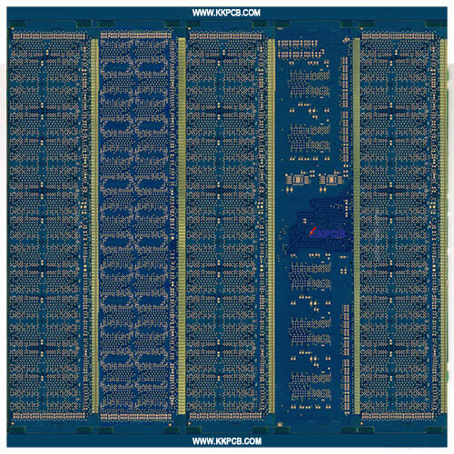
The customer is a globally leading manufacturer of communication equipment, specializing in the development and production of large-scale routers, switches, servers, and high-speed networking devices. As modern network communications demand increasingly high signal integrity, reliability, and thermal stability, the customer required an 36-layer PCB with low-loss material (S1000-2M) and advanced immersion gold plating to ensure stable signal transmission and long-term reliability.
2. Pain Points and Challenges of PCB Backplanes
In traditional communication PCB production, the customer faced the following key challenges:
- Signal Integrity Issues – In high-frequency and high-speed environments, poor impedance control led to signal attenuation and transmission errors.
- Insufficient Thermal Stability – Due to long-term high-load operations, standard PCB materials risked delamination, warping, or cracking.
- High-Density Routing Challenges – An 36-layer PCB requires ultra-fine trace width/space (3mil/3mil) and micro-vias (0.25mm), which traditional processes struggle to achieve with high yield.
- Surface Treatment Reliability – Standard OSP or immersion silver plating could not meet long-term oxidation resistance and contact stability requirements.
3. KKPCB Solution and Application Scenarios
To address the customer’s pain points, KKPCB provided an 36-layer S1000-2M ultra-low-loss material + immersion gold plating PCB backplane, ensuring:
- Ultra-Low Loss & Signal Stability – Using S1000-2M high-speed material (Dk=3.9, Df=0.008), signal loss is minimized in high-frequency environments, suitable for large-scale servers, base station routers, and 5G switching equipment.
- High Thermal Resistance Design – With a board thickness of 3.0mm and 70μm copper thickness, the PCB offers improved heat dissipation and mechanical strength, ideal for 24/7 continuous operation.
- Ultra-High Precision Manufacturing – 3mil trace width/space and 0.25mm minimum hole size meet high-density interconnection requirements, ensuring yield for complex PCBs.
- Long-Term Durability – Immersion gold surface finish (gold layer thickness: 0.05μm) provides excellent oxidation resistance and wear resistance, extending the product’s lifespan.

4. Conclusion
KKPCB’s 36-layer S1000-2M ultra-low-loss immersion gold backplane perfectly addresses the challenges of signal integrity, thermal stability, and high-density routing faced by communication equipment manufacturers. This solution has been successfully applied to the customer’s high-speed switches and core backbone routers, significantly improving the long-term stability and data transmission performance of the PCBs.
Through KKPCB’s advanced multilayer PCB manufacturing processes and high-quality raw materials, the customer has enhanced their product competitiveness, validating our leadership in the high-difficulty communication PCB industry.