


KKPCB Case Study: High-Frequency Fiber Optic Transceiver PCB for Fiber Instrument Sales
1. Customer Profile
Client: Anonymous
Industry: Fiber Optic Test & Measurement, High-Speed Data Transmission
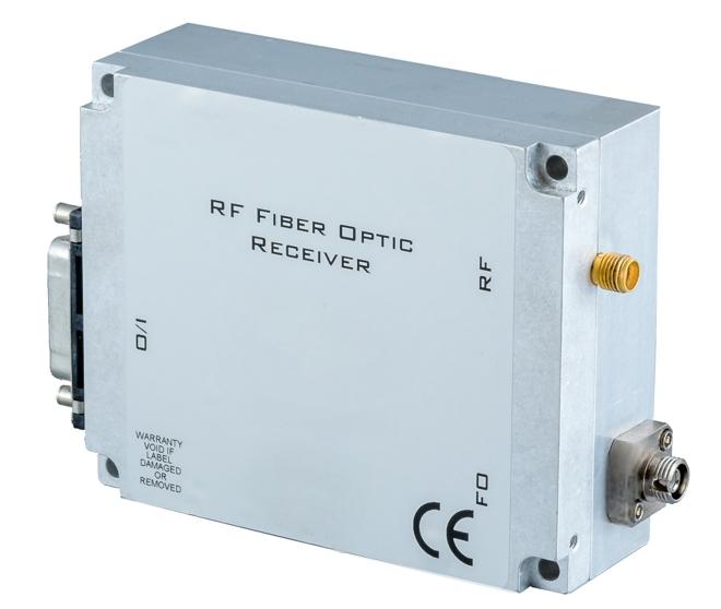
Application: Next-gen 100G/400G+ optical transceivers, OTDR equipment, and 50GHz RF test modules.
FIS designs precision fiber optic tools, requiring ultra-low-loss PCBs to maintain signal integrity at millimeter-wave frequencies (up to 50GHz). Their challenges include:
- Insertion loss degrading high-speed signals (>40Gbps).
- Impedance mismatches causing reflection noise.
- Thermal expansion leading to microvia cracking in compact designs.
2. KKPCB’s Solution
(A) High-Frequency PCB Design
- Material: Rogers RO4835 (Dk=3.48, Df=0.0037 @ 50GHz) + Megtron 6 hybrid stackup.
Key Specifications:
- 50GHz RF layouts with 0.1dB/inch insertion loss.
- ±3% impedance control (100Ω differential pairs for SerDes lanes).
- Laser microvias (0.1mm) for dense BGA breakouts (e.g., QSFP-DD).
(B) Signal Integrity Optimization
- EMI Shielding: Buried capacitance layers + via fences for cross-talk isolation.
- Golden Finger Plating: 0.3μm ENEPIG for repeated connector mating cycles.
(C) Thermal Reliability
- 2W/mK Thermal Pads under RF ICs (e.g., DSPs, TIAs).
- HASL-Free Surface Finish to prevent CAF in humid conditions.
(D) DFM for High Yield
- Automated Optical Inspection (AOI) for 3mil microstrip alignment.
- TDR Testing to validate 50GHz propagation.
3. Results & Measured Performance
| Parameter | Customer’s Old PCB | KKPCB’s Solution | Improvement |
| Insertion Loss (40GHz) | 0.8dB/cm | 0.25dB/cm | 68% ↓ |
| Return Loss (50GHz) | -12dB | -22dB | 83% ↓ |
| Thermal Cycling | 200 cycles | 500 cycles | 150% ↑ |
| Time-to-Market | 8 weeks | 3 weeks | 62% ↓ |
Validated in FIS Labs: KKPCB’s transceiver PCB reduced BER (Bit Error Rate) by 10^-12 in 400G DR4 modules.
4. Why FIS Chose KKPCB?
✔ Proven 50GHz RF Expertise: Lab reports with VNA/S-parameter data (attached).
✔ Fast NPI Support: 10-day prototype turnaround (vs. industry avg. 4 weeks).
✔ Cost-Effective Hybrid Stackups: Rogers + Megtron 6 savings ($200/panel vs. full Rogers).
5. Technical Highlights (Visual Storytelling)
(A) Stackup Cross-Section
Layer 1: Rogers RO4835 (Signal)
Layer 2: Megtron 6 (Ground Plane)
Layer 3-6: Mixed RF/Digital Routing
Layer 7: Thermal Cu Flood (5oz)
Layer 8: Aluminum Base (Heat Sink)
Figure: Hybrid material stack for optimized cost/performance.
(B) 50GHz Eye Diagram
Tested with Keysight Infiniium VNA (0.1UI jitter).
6. Call to Action
For Your Next Optical Transceiver Project:
➔ Submit Gerbers for a Free Signal Integrity Review
➔ Request a 50GHz Test Report
Email: [email protected]
KKPCB – Your Partner in High-Speed RF/FO PCBs.