Key Points of RF Circuit Board Design
RF circuit board design is a critical and often complex area of PCB engineering. While there are many uncertainties in theory, practical design rules can be followed to optimize performance. The following key points will focus on RF circuit board partitioning and design strategies.
1. Microvias in RF Design
Microvias are essential for connecting different layers on a PCB circuit board without generating electromagnetic interference. These vias usually have diameters between 0.05mm and 0.20mm and are categorized as:
- Blind vias: Connect surface layers to inner layers, used for surface-to-inner layer connections.
- Buried vias: Used within the inner layers, not extending to the surface, commonly used in multi-layer RF boards.
- Through vias: Pass through the entire board, providing internal connections or acting as component positioning points.
2. Partitioning Techniques for RF Boards
Proper partitioning of RF circuits is critical, especially to avoid interference between high-power RF amplifiers (HPA) and low-noise amplifiers (LNA). To achieve this:
- Physical partitioning: Separate high-power circuits from low-noise receiving circuits, ideally placing them on opposite sides of the PCB or designing them to work alternately.
- Electrical partitioning: Involves careful consideration of power distribution, RF routing, and grounding to minimize interference between sensitive circuits.
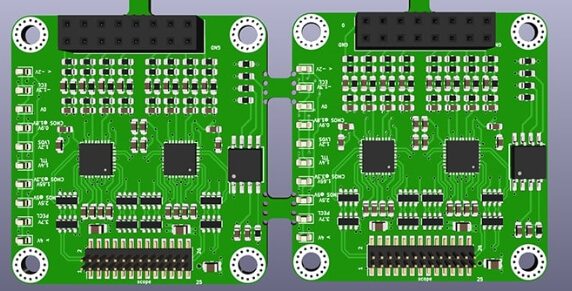
3. Physical Layout and Partitioning
Component layout is crucial for achieving an efficient RF design. Here are some tips:
- Place RF components close to each other to shorten the RF path.
- Keep RF inputs separate from outputs and away from high-power circuits.
- Minimize vias on RF paths to reduce inductance and signal loss.
- In multi-layer boards, use the second layer for grounding and route RF signals on the surface layer.
For mobile PCB designs, placing low-noise amplifier circuits on one side and high-power amplifiers on the other helps isolate noise and interference. Blind vias are often used to connect components while minimizing cross-talk.
4. Using Metal Shielding
When component separation is insufficient, metal shielding can be used to block RF energy from reaching sensitive areas. However, this comes with challenges:
- Increased manufacturing and assembly costs.
- Design restrictions due to the shape and size of metal shields.
- Difficulty in component replacement and increased board space requirements.
To ensure effective shielding:
- Route digital signals through the inner layers and RF signals through gaps in the metal shield, surrounded by ground areas.
- Use multiple vias to connect different signal layers to ground.
5. Power Decoupling
Power decoupling circuits are essential for reducing noise in RF designs. Decoupling is achieved through capacitors and inductors:
- Use capacitors of different values to filter noise at different frequencies. The capacitor closest to the chip (C4) should be selected based on its resonant frequency and connected as close as possible to the IC pin.
- Inductor (L1) helps isolate RF signals from the power line, preventing noise coupling.
Decoupling Layout:
- Place capacitors (C4, C3, C2) as close to each other and the IC pin as possible, with C4 nearest to the IC pin.
- Connect capacitors to the ground layer through vias close to the pads.
- Avoid placing inductors too close to each other to prevent mutual inductance and interference.
KKPCB conducts research on special processing technologies such as ordinary double-sided boards, thick copper circuit boards, high-frequency circuit boards, HDI circuit boards, rigid-flexible circuit boards, FPC flexible boards, buried blind hole circuit boards, and IC carrier boards. Provides PCB design, PCB layout, PCB prototyping and PCB assembly services.

