Issues to Consider in the Production of High-Frequency Microwave Printed Circuit Boards (PCBs)
With the continuous development of high-frequency electronic devices, especially in wireless networks and satellite communications, information products are becoming faster and higher in frequency, and communication products are moving towards large capacity and high-speed wireless transmission for voice, video, and data standardization. As a result, the next generation of products requires high-frequency substrates. The process technology for high-frequency PCB production is continuously improving to meet the diverse needs of users. Based on over ten years of experience in PCB production, this article will detail the key technical aspects and considerations for the production of high-frequency microwave PCBs.

Basic Requirements for High-Frequency Microwave PCBs
- PCB Substrate Material
When designing and simulating circuits, engineers must choose substrates with low dielectric constant and low dissipation factor to meet the actual signal transmission requirements. Therefore, when accepting customer orders, it’s essential to carefully verify the material parameters to ensure they meet design specifications. Common high-frequency materials include PTFE (Polytetrafluoroethylene), ceramic substrates, and polyimide (PI), each of which has unique electrical properties and application areas.- PTFE: Offers excellent electrical properties and low dielectric loss but is difficult to process and is relatively expensive.
- Ceramic substrates: Provide good thermal conductivity and electrical performance, suitable for stable high-frequency signal transmission, but have strict processing requirements.
- Polyimide (PI): Known for its excellent high-temperature resistance, often used in high-temperature and high-frequency applications.
- Precision of RF Transmission Lines
The transmission of high-frequency signals requires strict control of the characteristic impedance of the RF transmission lines. Generally, the tolerance for RF lines is ±20μm, and the edges must be smooth with no burrs or nicks. To ensure stable signal transmission, the characteristic impedance is typically controlled within ±10Ω. - Plating Requirements
The characteristic impedance of high-frequency microwave transmission lines directly affects signal transmission quality. The characteristic impedance is related to the thickness of the finished copper on the PCB, particularly for microwave boards with plated-through holes. Copper thickness uniformity must be strictly controlled to ensure stable electrical performance. - Mechanical Processing Requirements
The processing of microwave PCB materials differs significantly from that of conventional FR4 glass-epoxy materials. The required processing precision for high-frequency boards is much stricter, with the typical tolerance for the outer shape being ±0.1mm (with higher precision requirements of ±0.05mm). Accurate mechanical processing is critical to ensuring high-frequency board performance.
Key Considerations in the Production of High-Frequency Microwave PCBs
- CAM Data Processing
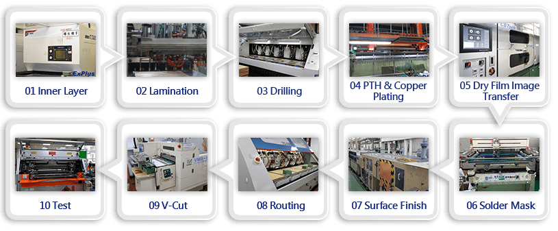
During CAM processing, it’s important to strictly follow the customer’s design requirements, especially regarding the transmission line tolerance. Appropriate process compensation should be made based on the tolerance requirements and the factory’s process capabilities to ensure that the production process aligns with the design specifications. - Material Cutting
For high-frequency dielectric materials, different cutting methods should be selected based on the material’s properties. Usually, milling and cutting methods are used to ensure that the material’s flatness and the board’s quality are not compromised. Special care should be taken when processing PTFE or other high-frequency materials to avoid material deformation or damage. - Drilling
Drilling is a critical step in high-frequency microwave PCB production. Drilling parameters must be adjusted based on different high-frequency dielectric materials, including drill bit geometry, cutting length, and spiral angle. New drill bits should be used to minimize burrs and ensure smooth hole walls with no defects.
Laser drilling technology can be used for precise small hole processing, improving hole accuracy and surface quality. - Copper Plating for Drilled Holes
Typically, chemical copper plating is used for through-holes in high-frequency microwave boards. Prior to plating, the holes must undergo a chemical cleaning process to remove debris. Plasma cleaning is used to treat the hole walls, improving the bonding strength between the copper layer and the substrate, preventing issues such as black holes or explosion holes, and enhancing the board’s reliability. - Pattern Transfer
The pattern transfer process is crucial to ensuring the accuracy of the PCB layout. Traditional exposure methods use mercury lamps to transfer images onto the PCB, while LDI (Laser Direct Imaging) technology uses lasers to directly image the pattern onto the copper surface. LDI provides higher resolution, making it suitable for fine-line production with a resolution down to 20 microns, which increases production yield. - Etching Process
The etching process requires strict control of process parameters, such as minimizing under-etching and over-etching, improving etching uniformity across the entire surface, and ensuring the edges of the lines are smooth and free of burrs.
Dry etching technology can be used to control the etching process more precisely, especially for fine lines and high-precision traces. - Solder Mask and Coating
The choice of solder mask material is crucial for high-frequency PCBs, as it directly impacts signal transmission quality. PTFE solder mask is commonly used as it helps reduce signal loss and improves signal integrity.
For special substrates, a segmented solder mask process may be required. For example, certain areas of the base material may not require solder mask, which requires the use of “base film” for solder mask application to ensure that only the necessary areas are coated. - Shaping Process
The shaping process for high-frequency microwave PCBs is similar to that for FR4 boards, mainly using CNC milling. However, due to the unique properties of high-frequency materials, specialized milling tools are required. Neutral cooling fluids should be used during milling, and the milling parameters, such as tool speed and feed rate, should be adjusted based on the material to ensure precise cutting.
Additional Considerations
- Soldering and Coating: When soldering, attention should be paid to factors such as solder pot temperature, wind pressure, and turn-over time. Care should also be taken during the clamping process to avoid leaving marks or scratches on the PCB surface.
- Temperature Control: Temperature control is essential in the production of high-frequency microwave PCBs. Stable temperature management during heat treatment and soldering processes ensures that materials do not deform or degrade in performance.

Conclusion
The production of high-frequency microwave PCBs is not only a technical challenge but also a rigorous requirement for craftsmanship and attention to detail. Each operation affects the final product’s quality, so every step must be carefully controlled to ensure that each board meets the highest quality standards. By consistently pursuing excellence in every process, we can stand out in a competitive market and meet customer demands for high-frequency products.
The production of high-frequency microwave PCBs is a complex and highly precise process involving multiple technical steps. Quality control at every stage is crucial to ensuring the final product meets industry standards. By paying close attention to every detail throughout production, manufacturers can ensure that the products will perform reliably and meet the highest quality expectations.

