Introduction to PCB Design
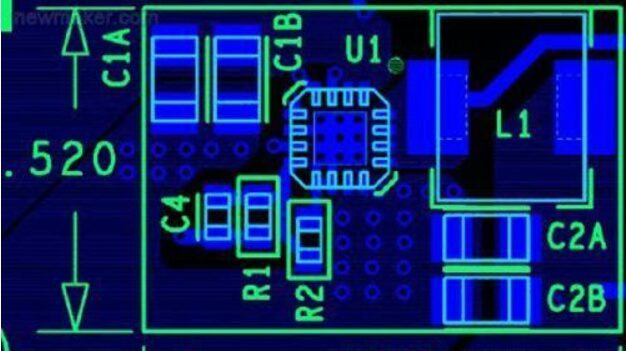
PCB design involves two critical stages: component layout and circuit connection wiring. The layout is the arrangement of circuit components within the PCB’s wiring area. A well-thought-out layout directly affects the ease of subsequent wiring and significantly impacts the PCB’s overall performance. In addition to meeting circuit functionality and performance requirements, a good layout considers manufacturability, inspection, and maintenance. Components should be placed evenly, neatly, and compactly, ensuring that leads and connections are short, minimizing interference and signal transmission delays.
When organizing functional circuit units, it’s essential to consider circuit flow. Signals such as input/output, high/low voltage, and digital/analog parts should be kept apart to reduce interference. High-frequency and heat-generating components must be strategically separated to minimize electromagnetic interference and ensure proper thermal management.
PCB Design Steps
Designing the circuit schematic is the foundation of PCB design. The steps are as follows:
- Open the schematic editor (e.g., Protel DXP).
- Set schematic layout size and design boundaries.
- Place components from the component library onto the work plane.
- Connect components according to the design.
- Adjust layout post-wiring for optimal performance.
- Save schematic and export the document.
- Print output for review or manufacturing.
PCB Layout Checklist
- Board size: Ensure consistency with design specifications.
- Component arrangement: Should be balanced and neatly organized.
- Conflict check: Verify that components and levels don’t interfere.
- Accessibility: Components requiring frequent use should be easy to access.
- Thermal management: Ensure proper spacing between heat-sensitive and heat-generating components.
- EMI considerations: Assess interference-related issues to minimize crosstalk.
PCB Design Sequence
PCB design begins with system specifications, covering the overall system’s function, size, and cost constraints. The next steps involve designing a functional block diagram, breaking the system into individual PCB boards for modular design and system upgrades.
Key design decisions include:
- Packaging technology and PCB size.
- Special component placement.
- Separation of digital and analog circuits, along with grounding considerations.
General PCB Design Principles
When laying out components, consider the following:
- Minimize high-frequency interference: Shorten the paths between high-frequency components.
- High-voltage safety: Increase distances between components with significant voltage differences.
- Thermal components: Heat-generating parts should be mounted on the chassis or away from heat-sensitive areas.
- Adjustable components: Potentiometers, switches, etc., should be placed for easy adjustment.
Wiring Guidelines
PCB wiring follows several rules to ensure functionality and reliability:
- Signal wires: Keep input and output wires separated to avoid feedback loops.
- Wire width: Choose appropriate widths based on the current. For digital circuits, widths of 0.02-0.3 mm are typical, while power lines should be wider.
- Bends: Use arc-shaped bends to avoid electrical issues, especially in high-frequency circuits.
Pads, Vias, and Silkscreen Layers
- Pads: The hole size should be slightly larger than the component leads. For high-density digital circuits, the pad diameter should be minimal to save space.
- Vias: Properly size vias based on current requirements. Special attention is needed for power layers.
- Silkscreen layer: Ensure that component labels are readable and not obscured during assembly.
PCB Design Considerations
- Avoid critical signals at the board’s edge.
- Ground wire placement: Keep the ground wire far from the signal lines and as continuous as possible to reduce inductance.
- Wire widths: For general traces, maintain a minimum width of 0.2mm, but increase this for power lines.
- Design for manufacturability: Components that generate heat should have windows for proper cooling and assembly considerations.
Skills for Effective PCB Design
- Grid accuracy: During layout, use a larger grid for big components and a smaller grid for small parts.
- Component arrangement: Maintain symmetry and compact layouts for signal integrity and manufacturability.
- Wiring strategy: Keep wires short to minimize inductance and allow better grounding for low-impedance paths.
By following these optimized PCB design principles, you ensure the functionality, performance, and manufacturability of your printed circuit boards.
As a leading PCB manufacturer, members of our printed circuit board (PCB) design service team are practical partners working with you on every project and can help you achieve your goals at any time. They can complement your engineering expertise, which helps speed up time to market, reduce the time from concept to production, and ensure that quality is integrated into the manufacturing process to maximize your profits.


