


Internet of Things (IoT)
- Home
- Internet of Things (IoT)
IoT and Wearables PCB Assembly service
IoT (Internet of Things) is rapidly gaining prominence and pervading our modern world. Its presence spans multiple sectors and domains, including smart homes, wearable devices, industrial automation, and smart cities. This technology revolutionizes the way we live by enhancing convenience, personalization, safety, sustainability, and efficiency. Through interconnected devices, IoT simplifies daily routines, automates tasks, and offers personalized experiences tailored to individual preferences. As an expert in IoT electronics manufacturing, KKPCB takes pride in providing customers with reliable and customized IoT devices and solutions that improve people’s lives. With our expertise, we contribute to creating a connected and convenient world through the power of IoT.
Application of IoT PCB
Smart Home
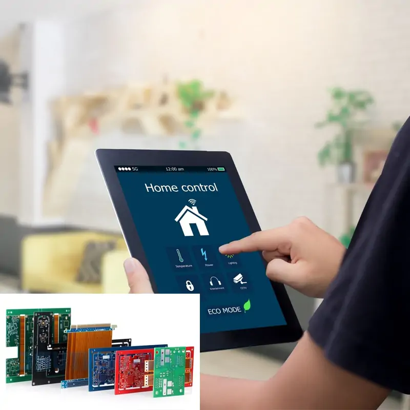
IoT PCB can be used in smart home devices, such as smart lamps, smart sockets, smart curtains, etc., to realize remote control and intelligent management of devices through technologies such as sensors and communication modules.
Industrial Automation
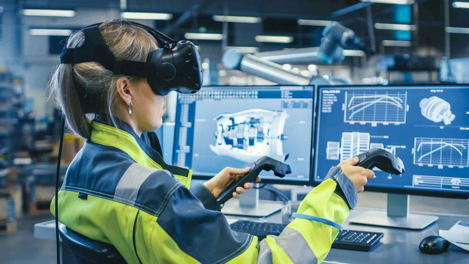
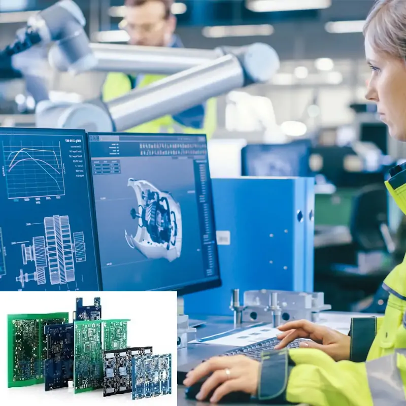
IoT PCB can be used in the field of industrial automation, such as intelligent warehouse logistics management, intelligent manufacturing, etc., through technologies such as the Internet of Things and big data, to achieve comprehensive monitoring and intelligent management of the production process.

Smart City
IoT PCB can be used in the construction of smart cities, such as smart street lights, smart parking, etc., to realize intelligent management and refined services of urban facilities through technologies such as the Internet of Things and cloud computing.

Medical Health
IoT PCB can be used in the field of medical health, such as smart health monitoring, smart medical equipment, etc., through sensors, communication modules and other technologies, to achieve remote monitoring of patients and intelligent management of medical services.

Agricultural Intelligence
IoT PCB can be used in the field of agricultural intelligence, such as intelligent irrigation, intelligent farming, etc., through technologies such as the Internet of Things and big data, to achieve intelligent management and refined services for agricultural production.

Intelligent transportation
IoT PCB can be used in the field of intelligent transportation, such as intelligent traffic lights, intelligent vehicle equipment, etc., through technologies such as the Internet of Things and cloud computing, the intelligent management of transportation facilities and the realization of intelligent transportation can be realized.
Features of Our IoT PCBs
Multifunctional:
IoT PCB can accommodate and integrate a variety of sensors, signal processing, communication and data storage devices, supporting various types of data acquisition and processing.
Space saving:
IoT PCB adopts compact design, which can put more components and functions on a small size circuit board.
The manufacturing cost of IoT PCB is relatively low because it can integrate multiple components and functions on a small circuit board, which reduces the manufacturing cost.
High performance:
IoT PCB adopts high-precision, high-speed and high-density circuit design, which provides faster data transmission speed, lower power consumption, higher reliability and larger capacity.
Customizable:
IoT PCB can be customized according to customer needs to meet the requirements of various application scenarios.
Highly integrated:
IoT PCB has higher integration and diversified functions, which can realize more efficient data collection and processing, and is an important part of IoT devices.
- Connecting devices: IoT PCBs can connect various IoT devices, enabling them to communicate and exchange data with each other.
- Data acquisition and processing: IoT PCB can integrate multiple sensors and other data acquisition devices to realize real-time acquisition and processing of various data such as environment, location, temperature, humidity, and pressure.
- Realize remote control: Through IoT PCB, IoT devices can be remotely controlled, such as controlling a home automation system through an application on a smartphone or computer.
- Support for big data: IoT PCBs can process large amounts of data to support data analysis and decision-making to improve equipment operations and optimize production efficiency.
- Improve production efficiency: Through IoT PCB, production equipment can monitor and analyze data in real time, realize the automation and optimization of the production process, and improve production efficiency and quality.
Why Choosing KKPCB For Your IOT PCBs
High Quality
Our IoT PCBs use high-quality materials and advanced manufacturing processes, which guarantee high-quality manufacturing and stable performance.
Customized services
We provide customized IoT PCB services that can meet your specific needs, including size, shape, circuit design, etc.
Fast delivery
We have a fast production and delivery cycle, and can provide IoT PCB products in the shortest time.
Affordable
Our IoT PCB prices are good value for money and can meet your budget needs.
Professional technical support
We have a technical professional team that can provide high-quality technical support and solutions to help you solve any problems.
Reliability guarantee
Our IoT PCB products have high reliability and long life, which can meet your long-term use needs, and we will also provide quality assurance and after-sales service.
Internet of Things (IoT) PCB
Frequent Questions
An Internet of Things (IoT) PCB is a specialized printed circuit board designed to enable connectivity and functionality in smart devices. It features compact, energy-efficient designs with integrated communication modules and sensors, robust construction for varying environments, and security measures to protect data. IoT PCBs are essential for applications across smart homes, wearable technology, industrial automation, agriculture, and healthcare, facilitating devices that collect, transmit, and receive data over the internet.
IoT PCBs are used in a variety of applications such as smart home devices, wearables, industrial automation, agriculture, healthcare, smart cities, retail, and logistics. They enable connectivity, real-time data collection, and automation, enhancing efficiency and functionality in these sectors. IoT PCBs facilitate remote control, monitoring, and optimization of systems, driving innovation and improving operational performance across diverse industries.
Quality assurance for IoT PCBs involves ensuring that designs meet specifications, components are high-quality, and manufacturing processes adhere to standards. Key aspects include verifying soldering quality, using automated optical inspection (AOI), conducting in-circuit and functional testing, and performing environmental and stress tests. Compliance with electromagnetic compatibility (EMC) and electromagnetic interference (EMI) standards, security measures, traceability, and continuous improvement processes are also essential to ensure the reliability, performance, and safety of IoT devices.
In IoT PCB design, crucial factors include ensuring connectivity with various communication protocols, optimizing for low power consumption, and accommodating compact sizes. Effective thermal management, signal integrity, and mechanical durability are essential for reliable operation. Environmental resistance, compliance with standards, and incorporation of security features are also critical. Additionally, planning for comprehensive testing and ensuring scalability and flexibility for future upgrades are important for creating robust and adaptable IoT devices.
Internet of Things (IoT) PCBs are characterized by their support for various communication protocols, compact and energy-efficient design, and integration of multiple functions such as sensors and microcontrollers. They include robust thermal management, maintain signal integrity, and offer durability and environmental resistance. Additionally, they incorporate security features to protect data, allow for scalability and future upgrades, and facilitate easy integration into interconnected systems, ensuring reliable and efficient performance in diverse IoT applications.
Internet of Things (IoT) PCB assembly types include Surface-Mount Technology (SMT) for high-density designs, Through-Hole Technology (THT) for robust connections, and Mixed Technology for combining both methods. Flexible PCBs offer adaptability for space-constrained designs, while Rigid-Flex PCBs provide a balance of rigidity and flexibility. Hybrid PCBs integrate traditional materials with advanced technologies for specialized functions. Each type is selected based on the specific needs for component density, flexibility, durability, and integration in IoT devices.
IoT PCB products are essential because they enable connectivity and integration in smart devices, enhancing their functionality and efficiency. They facilitate data collection and analysis, improve user experiences, and drive innovation across various sectors. Additionally, IoT PCBs support scalable, adaptable designs and incorporate security features to protect against cyber threats, making them crucial for the advancement and effectiveness of IoT applications.
For Internet of Things (IoT) PCB assembly, essential files include Gerber files for layout details, Bill of Materials (BOM) for component specifications, pick and place files for accurate component placement, and assembly drawings for visual guidance. Stencil files are needed for solder paste application, while design files provide the electrical and physical layout. Additionally, test plans ensure proper functionality and quality, fabrication drawings detail manufacturing specifications, and material specifications confirm the required performance standards. These files collectively ensure precise production, accurate assembly, and reliable performance of IoT PCBs.