Innovative printing solutions for front-end RF module packaging
5G communication has the technical characteristics of high frequency, broadband, and high power density, and its demand for RF front-end devices has also increased significantly. At the same time, in order to control the volume of the assembled device, the modularization of the RF front-end is inevitable. The RF front-end module integrates the power amplifier (PA), filter (SAW, TF-SAW BAW, etc.), antenna, switch (Switch) and low noise amplifier (LNA), passive devices, etc. in one module. Because PA, antenna, switch, and LNA are relatively mature and have been domestically produced, and filter technology has long been controlled by foreign companies, it has become a technical bottleneck for 5G RF modules. In recent years, domestic filters have gradually been certified by major OEMs, making domestic RF front-end modules possible. For packaging and testing plants, this is both an opportunity and a new challenge.
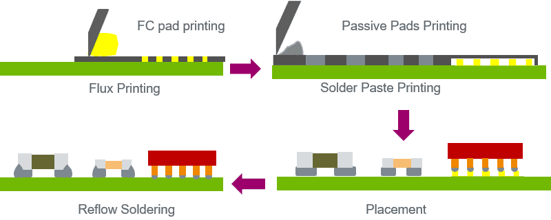
In the traditional RF module packaging process, the components are mounted using SMT technology. The main process steps are shown in Figure 1 (the schematic diagram omits the SPI and AOI processes)

Figure 1: Traditional process steps
As shown in Figure 1, the process flow is to first use the first printer to print flux on the flip chip position, and then use the second printer to print solder paste on the passive device position. However, a stepped steel mesh is needed to avoid the position where the flux has been printed to prevent the second printing from affecting the flux. Therefore, two printers, two steel meshes, and two materials (flux and solder paste) are required in this process.
Because product design requires the realization of complex and more powerful module functions in a smaller package size, high-density mounting must be performed inside the module. However, this brings unprecedented challenges to the SMT process, as shown in Table 1.
| Challenges and Problems | Problem Analysis | |
| Challenges of product design | Smaller passive component size | As small as 008004 |
| Smaller chip-to-chip spacing | Breaking through the existing design limits | |
| Smaller bump spacing | The gap in cu-pillar is as narrow as 130-150um or even narrower | |
| Process and material challenges | SPI’s flux recognition capability for printing | The color is lighter and the device cannot recognize it |
| Bump solder joint open circuit (None-Wet-Open) | Bump coplanarity, substrate deformation, insufficient flux |
Table 1: Challenges in module packaging
To address the above challenges, Heraeus developed an all-in-one printing process, as shown in Figure 2.

Figure 2: One-shot printing process
As can be seen from Figure 2, this process eliminates the traditional process of flux printing and adopts one-time solder paste printing to cope with all types of devices, which can greatly save equipment investment and process time. At the same time, since SPI has better recognition of solder paste, the new process can also avoid the problem that SPI cannot recognize flux. However, this process needs to be able to cope with the following specific challenges:
▪ The window size of the steel mesh corresponding to 008004 is 90-100um or even smaller. Can the new process ensure the consistency of solder paste printing?
▪The spacing between the copper pillars of some FC chips is as narrow as 130-150um. Can the new process control the stability of the tin amount to prevent tin bridging? We designed an experimental verification:
1. Steel mesh: ultra-thin electroformed steel mesh
2. Solder paste: Two types of No. 7 powder solder paste WS5112 T7 and AP520 T7
The details are shown in Table 2.
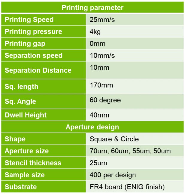
Table 2: Printing parameters and steel mesh design
The printing results are shown in Figure 3.
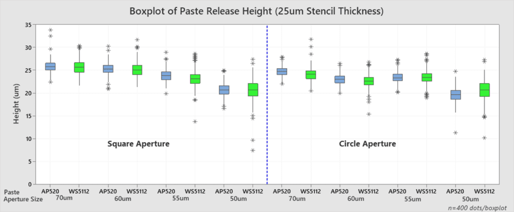
Figure 3: SPI test results
As can be seen from Figure 3, above the aperture size of 50um, the height of the printed solder paste is very consistent, and the solder paste release heights of square holes and round holes are also relatively close; when the aperture is 50um, the solder paste release height drops significantly.
The physical inspection and defect statistics after printing are shown in Figure 4, Figure 5 and Table 3.
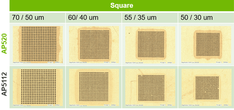
Figure 4: Printed product with square openings
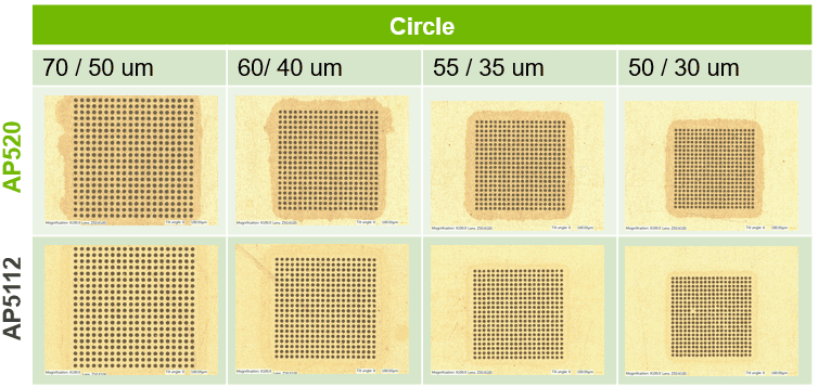
Figure 5: Printed object with circular openings

Table 3: Statistics of printing results
(Note: LS = line space, SO = stencil opening)
As can be seen from Table 3, AP520 T7 has a larger process window and can support a minimum aperture size (SO) of 55um, while WS5112 T7 starts to have insufficient solder paste when the aperture size is 60um or below.
In summary, No. 7 powder solder paste has good printability and can meet the requirements of ultra-fine spacing.
Bump solder joint open circuit (Non-wet-open): Usually bump coplanarity, substrate deformation, and insufficient flux activity are some of the reasons for bump solder joint open circuit. When the above situation occurs, a certain thickness of solder paste is printed on the pad of the substrate. The solder paste can maintain the printed shape to fill the large gap between the bump and the pad caused by the large difference in bump coplanarity or the warping of the substrate, thereby avoiding bump solder joint open circuit after reflow soldering. Flux does not contain metal components and has good fluidity after printing. It is difficult to maintain the shape after printing, so flux does not have such a function. To improve this problem, the customer used WS5112 T7 solder paste for verification.
Client’s case sharing Test Vehicle: SiP package contains 3 flip-chips and 18 01005 passive components. 4 test groups, 80 solder joints in each group, a total of 320 test points.
▪ The largest opening of FC steel mesh is 125x720um,
▪The smallest opening is 70um,
▪Minimum opening gap (edge to edge of adjacent openings) 40um
▪The thickness of electroformed steel mesh is 30um
▪The solder pastes used are Heraeus WS5115 T7 and competitor products A and B.
The test results are shown in Table 4:
| CTQ | A | B | HeraeusWS5112 |
| Tinning yield | 55.30% | 45% | 99.10% |
| (Defect %) | (143/320,44.7%) | (176/320,55%) | (3/320,0.9%) |
| Void yield | 0% | 94.10% | 100% |
| (max 9% area) | (320/320) | (19/320) | (0/320) |
| Average cavity area | 22.50% | 8.40% | ~0% |
Table 4: Comparison of test results
As shown in Table 4, the test results show that the defective tin connection rates of competing products A and B are as high as 44.7% and 55%, while that of WS5112 is only 0.9%. The void yield performance of A is 0, B is 94.1%, and WS5112 is 100% (see Figure 6 X-RAY photo). The most stringent thing in this test is the 40um opening gap, which has exceeded our recommended lower limit (minimum opening 70um, opening gap 50um). WS5112 has very significant advantages compared with competing products A and B. .
In the results of the printing test shown above, when the minimum opening is 70um and the minimum gap is 50um, there is no bridging problem in both square and circular openings. Combined with the results of this test, we know that the minimum opening gap that WS5112 can support is 50um. At the same time, the non-wet-open defect rate is reduced by 600 times (ppm level), and the actual slice diagram is shown in Figure 6.
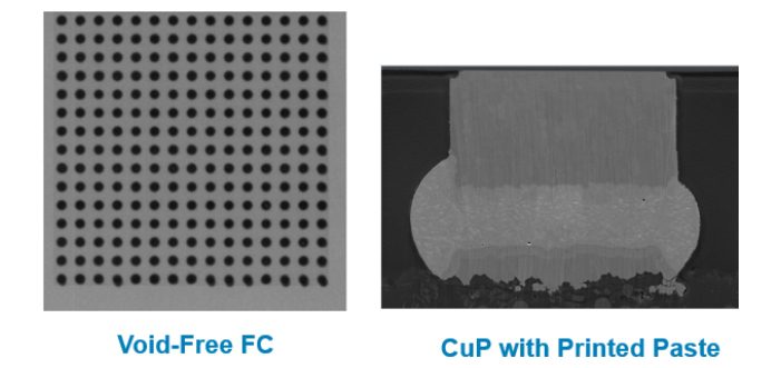
Figure 6: Void performance
A one-shot printing solution can bring many benefits:
1. Fewer process steps: Ultrafine powder solder paste is combined with ultra-thin steel mesh to improve printability at finer pitches and can replace the use of flux.
2. Lower cost: Eliminates flux, additional steel mesh, printing equipment
3. Reduce defective rate: Reduce open PCB circuit problems caused by substrate warping and large differences in solder ball coplanarity
One-shot printing is a mature process solution that has been mass-produced by major manufacturers at home and abroad. Heraeus can provide matching materials and professional services.
| WS5112 | AP520 |
| Welco™ Type 7 | Welco™ Type 7 |
| SAC305 | SAC305 |
| DI water plus surfactant cleaning | DI water cleaning |
| Application target: 120um pitch and above | Application target: 90um pitch and above |
| Low void rate | Low void rate |
| No splash Wuxi beads | No splash Wuxi beads |
| 8 hours printing life | 12 hours printing life |
| Valid for 3 months | Valid for 4 months |
Table 5: WS5112 and AP520 information comparison table
The basic information of the two solder pastes is shown in Table 5 above. If you have any requirements or questions, please contact Heraeus Electronics.s Electronics.


