PCB Design for Motor Driver ICs: Key Techniques for Thermal Management and Power Handling
Motor driver ICs handle high currents and dissipate substantial heat, so efficient PCB design is essential to ensure proper heat dissipation and reliable performance. Below are some best practices for designing a robust PCB for motor driver ICs.
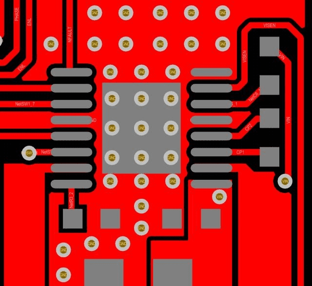
1. Use Large Copper Areas of PCB layout
Copper plays a vital role in heat dissipation because it has excellent thermal conductivity, unlike FR-4 PCB substrate, which is a poor conductor of heat. Here’s how to use copper effectively:
- Increase Copper Thickness: Using thicker copper (like 2-ounce foil) improves heat conduction, but it’s expensive and can limit fine geometry. A more practical option is to use 1-ounce copper.
- Solid Copper Planes: On multi-layer PCBs, internal copper planes help spread heat, but since they’re buried inside the board, heat can get trapped. To resolve this, designers place copper pours on outer layers and link them to internal layers using thermal vias (explained later).
- Copper Pours on 2-Layer PCBs: Spreading heat on a 2-layer PCB is more difficult since traces and components cut through the copper. Copper pours should be placed on both sides of the board and connected with vias to maximize heat dissipation.
2. Optimize Trace Widths
Since motor drivers handle large currents (often exceeding 10A), the trace width must be wide enough to avoid excessive resistance and prevent traces from overheating or acting as fuses. Here are the essential points:
- IPC-2221 Guidelines: This standard provides recommended trace widths based on current, copper thickness, and allowable temperature rise. For instance, a 10A current on 1-ounce copper requires a 7mm-wide outer-layer trace, but on 2-ounce copper, only 3.5mm is needed.
- Short, Wide Traces: While it seems impractical to run 10A through a small IC pad, designers widen traces right after the pad. This way, the narrow trace length is short, and most of the current flows through the wider copper area, which acts as a heatsink.
- Inner-Layer Traces: Traces on inner layers require double the width of outer-layer traces because heat dissipation is limited by the surrounding FR-4 material.
Recommended Trace Widths (Based on IPC-2221)
| Current | 1oz Copper (Outer Layer) | 1oz Copper (Inner Layer) | 2oz Copper (Outer Layer) | 2oz Copper (Inner Layer) |
|---|---|---|---|---|
| ≤ 1A | 0.6mm | 1.2mm | 0.3mm | 0.6mm |
| 2.5A | 1mm | 2mm | 0.5mm | 1mm |
| 5A | 2.5mm | 5mm | 1.2mm | 2.5mm |
| 10A | 7mm | 14mm | 3.5mm | 7mm |
3. Use Thermal Vias
Thermal vias conduct heat from the surface of the PCB to internal layers, helping to dissipate heat trapped inside the PCB.
- Plated Vias: Vias are small plated holes that typically connect signal layers, but they also play a role in transferring heat. Vias with larger diameters have lower thermal resistance, so more copper is used for effective heat transfer.
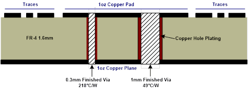
- Via Size and Placement: Large vias conduct heat well but may cause solder wicking (where solder seeps into the hole), creating a poor solder joint. To avoid this:
- Use smaller via holes (but more of them) to minimize solder wicking.
- Tent the vias: Cover them with solder mask on the backside, preventing solder from flowing in.
- Use via-in-pad techniques, but ensure the vias are either filled or capped to avoid solder wicking.
- Avoid Thermal Reliefs: Thermal reliefs (connections with narrow “spokes” to copper pads) are typically used for solderability, but in the case of thermal vias, this reduces heat transfer efficiency. Direct connections to copper planes are preferred for effective heat dissipation.

4. Soldering Exposed Pads
Many IC packages (like TSSOP and QFN) have an exposed thermal pad under the chip. Soldering this pad correctly is essential for thermal performance.
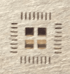
- Use a Stencil for Solder Paste: Solder paste is applied to the thermal pad using a stencil, but a single large opening can result in too much solder, causing the device to “float” or lift during reflow.
- Apply Solder Paste in Patterns: Instead of one large opening, create a pattern of multiple smaller deposits of paste (e.g., dots, squares, or smaller patches) to allow for better venting of flux gases.
- Consult SMT Process Engineers: Check with the assembly engineers to ensure proper stencil design and solder volume to avoid reliability issues like solder voiding (air gaps in the solder joint) and floating components.
5. Place Components Strategically
Proper component placement affects heat dissipation and signal integrity. Key guidelines include:
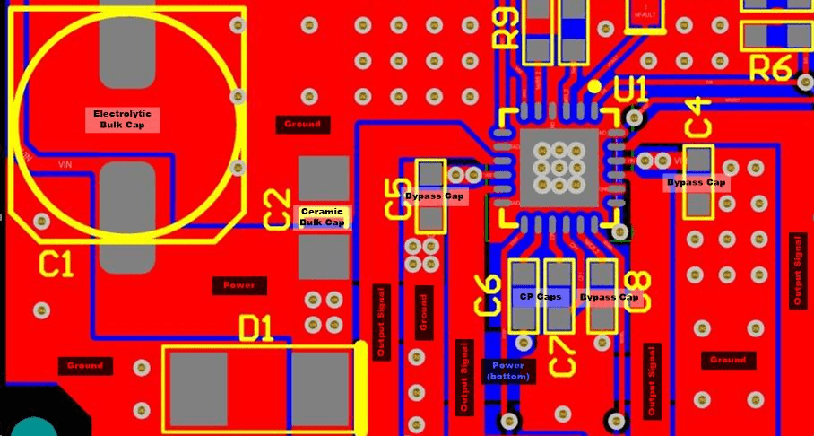
- Bypass Capacitors: Place capacitors close to the power pins of the motor driver IC. Use low-ESR capacitors for high-speed bypassing and filter noise.
- Bootstrap and Charge Pump Capacitors: These capacitors should be placed as close to the motor driver IC as possible, reducing the risk of noise and parasitic inductance issues.
- Place Bulk Capacitors: Use bulk capacitors near the IC to stabilize power supply voltages and smooth out high current transients.
- Power and Ground Paths: Power traces and ground paths should be short and wide to handle high currents and maintain low impedance. Use multiple vias to connect ground planes.
6. General Design Recommendations
- Increase the Copper Area: Use as much copper as possible for ground and power planes.
- Reduce Current Crowding: Avoid sharp corners or abrupt changes in trace width. Use smooth, gradual transitions.
- Use Heat Sinks and Copper Pours: On high-power circuits, consider adding heat sinks or larger copper pours to aid heat dissipation.
- Simulate Thermal Performance: Use simulation tools to predict the PCB’s thermal performance under operating conditions, and make design changes before production.
Conclusion
Designing a PCB for motor driver ICs requires thoughtful consideration of thermal management, current handling, and component placement. By following these design practices—like using large copper areas, wide traces, thermal vias, and proper soldering techniques—engineers can ensure the PCB remains cool, efficient, and reliable. For optimal results, always consult SMT process engineers and PCB fabricators for guidance on manufacturability.


