Comprehensive Guide to Types and Characteristics of Ceramic Substrates
In this guide, we’ll explore the main types of ceramic substrates and the manufacturing processes that shape their unique characteristics.
1. Classification by Material
1.1. Alumina (Al₂O₃) Substrate
Alumina (Al₂O₃) is the most widely used material for ceramic substrates due to its excellent combination of mechanical strength, thermal conductivity, chemical stability, and cost-efficiency. With its abundant raw material supply, alumina is well-suited for various manufacturing methods and customizable shapes, including 3D designs. Its versatility makes it a dominant material in microelectronics, power electronics, hybrid microelectronics, and power modules.
1.2. Beryllium Oxide (BeO) Substrate
Beryllium Oxide (BeO) substrates exhibit exceptional thermal conductivity, even higher than metallic aluminum. This makes them ideal for high-power applications. However, their use is limited due to the material’s toxicity, requiring special handling precautions. BeO is typically used in niche applications where high thermal performance is crucial.
1.3. Aluminum Nitride (AlN) Substrate
Aluminum Nitride (AlN) substrates have two standout features: high thermal conductivity and a thermal expansion coefficient that matches that of silicon. This property makes AlN particularly valuable in semiconductor packaging. However, its cost is significantly higher than that of alumina, and the manufacturing process requires strict quality control to maintain thermal conductivity consistency. Despite these challenges, AlN’s superior properties have led to growing adoption in high-power electronic systems.
2. Classification by Manufacturing Process
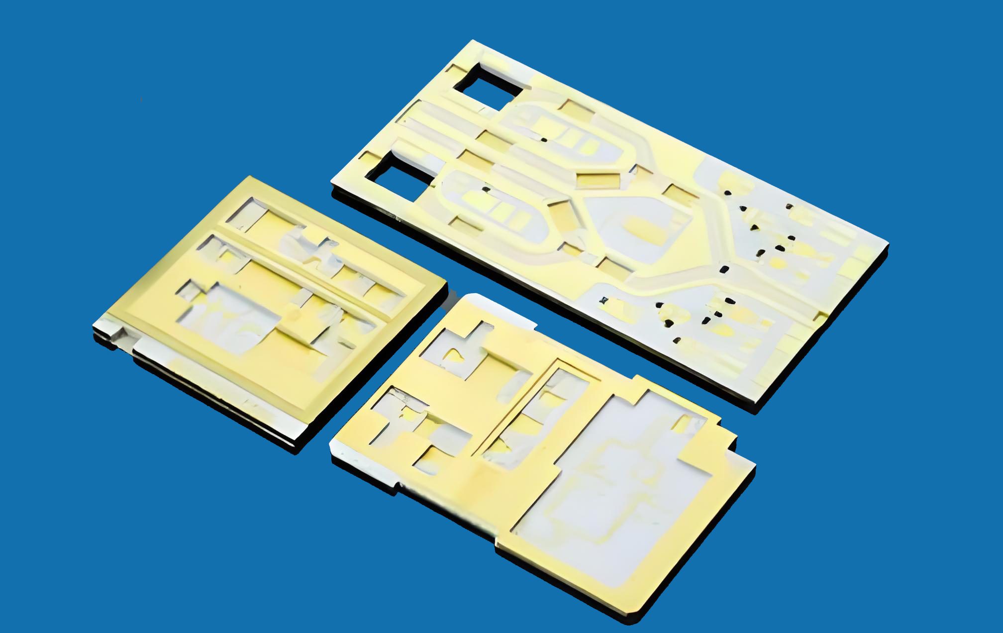
The current mainstream ceramic heat dissipation substrate types include HTCC, LTCC, DBC, DPC, and LAM. Each process offers unique characteristics that influence the final product’s performance and applications.
2.1. HTCC (High-Temperature Co-fired Ceramic)
HTCC, or High-Temperature Co-fired Ceramic, is produced by firing at temperatures of 1300°C to 1600°C. Unlike LTCC, HTCC does not use glass additives in the ceramic powder, resulting in a more robust product. The manufacturing process involves drilling via holes, screen printing circuits with high-melting-point metals (like tungsten or molybdenum), and finally co-firing at high temperatures. HTCC substrates are known for their high mechanical strength and durability, but the limited choice of conductor materials restricts their use in certain applications.

2.2. LTCC (Low-Temperature Co-fired Ceramic)
LTCC, or Low-Temperature Co-fired Ceramic, is manufactured by mixing ceramic powder with 30-50% glass additives. This allows it to be fired at a lower temperature of 850°C to 900°C. The LTCC process involves screen-printing metal circuits (such as silver, gold, or copper) on individual ceramic layers, which are then stacked and co-fired. This technique enables the use of low-resistance metals, making LTCC suitable for high-frequency circuits and multi-layer designs.
2.3. DBC (Direct Bonded Copper)
DBC technology directly bonds copper to a ceramic substrate, such as alumina (Al₂O₃) or aluminum nitride (AlN). The process involves heating the copper and ceramic to form a eutectic bond at a temperature of approximately 1065°C – 1083°C. During the bonding process, copper reacts with oxygen to create a Cu-O eutectic layer, which ensures a firm bond between the copper and ceramic. DBC substrates are widely used in power modules and IGBT modules due to their high thermal conductivity and excellent electrical insulation.
2.4. DPC (Direct Plated Copper)
DPC, or Direct Plated Copper, involves vacuum sputtering a copper film onto the ceramic substrate’s surface, followed by photolithographic patterning and copper plating to build up circuit layers. The precision of the DPC process allows for the creation of high-density interconnects (HDI) with fine pitch and small line/space dimensions (as fine as 20 μm). DPC substrates are widely used in LED modules, high-frequency RF devices, and advanced semiconductor packages.
2.5. LAM (Laser Activation Metallization)
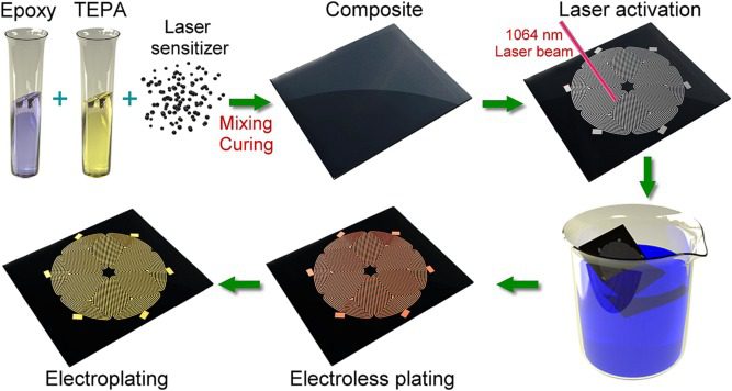
LAM, or Laser Activation Metallization, is a unique technology developed in collaboration with Huazhong University of Science and Technology’s National Optoelectronics Laboratory. This process uses high-energy laser beams to activate ceramic and metal ions, forming a strong bond between the ceramic substrate and the metal layer. LAM allows for the creation of thick copper layers ranging from 1 μm to 1 mm, which provides unmatched flexibility in circuit design. Key features of LAM include:
- High thermal conductivity: Replacing the insulation layer with a ceramic layer improves overall thermal performance.
- Improved thermal expansion matching: LAM’s thermal expansion coefficient is close to that of semiconductor materials, preventing stress-induced cracking.
- High adhesion strength: The metal layer’s adhesion strength exceeds 45 MPa, ensuring robust connections.
- Customizable copper layer thickness: Ranges from 1 μm to 1 mm, unlike traditional DBC, which is limited to 100 μm to 600 μm.
Summary of Key Substrate Types
| Substrate Type | Thermal Conductivity | Strength | Manufacturing Cost | Primary Use |
|---|---|---|---|---|
| Alumina (Al₂O₃) | Moderate | High | Low | Power electronics, LED modules |
| Beryllium Oxide (BeO) | High | High | High (limited use) | Niche high-power applications |
| Aluminum Nitride (AlN) | Very High | Moderate | High | Semiconductor packaging, power modules |
| Manufacturing Process | Thermal Conductivity | Complexity | Cost | Applications |
| HTCC | Moderate | High | High | Automotive, aerospace, harsh environments |
| LTCC | Low to Moderate | High | High | High-frequency RF circuits, multi-layer designs |
| DBC | High | Moderate | Moderate | IGBT modules, power modules, inverters |
| DPC | Very High | Very High | High | LEDs, high-density interconnects (HDI), RF devices |
| LAM | Very High | Very High | High | 3D circuit boards, aerospace, power devices |
Conclusion
Ceramic substrates play a critical role in modern electronics, offering exceptional thermal performance, mechanical strength, and customization options. Alumina remains the most widely used material due to its affordability and versatility, while aluminum nitride is favored for applications requiring higher thermal conductivity. The choice of manufacturing process—whether HTCC, LTCC, DBC, DPC, or LAM—will depend on the specific needs of the application, including power electronics, electronic packaging, hybrid microelectronics, and multi-chip modules. With their outstanding thermal conductivity, mechanical stability, and electrical insulation properties, ceramic substrates play a pivotal role in developing advanced electronic devices.
As new technologies like LAM continue to evolve, the future of ceramic substrates looks promising. The combination of improved thermal conductivity, flexible circuit design, and stronger adhesion means that LAM-based ceramic substrates could become the go-to choice for high-power electronic devices, LEDs, and next-generation semiconductor packaging.

