How to optimize PCB design to maximize the performance of superjunction MOSFETs
Based on recent trends, improving efficiency is a key goal, and the trade-off of using slow switching devices for better EMI is not worth it. Superjunctions can improve efficiency in applications where planar MOSFETs struggle. Superjunction MOSFETs significantly reduce on-resistance and parasitic capacitance compared to traditional planar MOSFET technology. The significant reduction in on-resistance and reduced parasitic capacitance, while helping to improve efficiency, also produces fast switching transitions of voltage (dv/dt) and current (di/dt), forming high-frequency noise and radiated EMI.
To drive fast switching superjunction MOSFETs, it is important to understand the impact of package and PCB layout parasitics on switching performance, as well as PCB layout adjustments for using superjunctions. Superjunction MOSFETs with a breakdown voltage of 500-600V are mainly used. Among these voltage ratings, the industry standard TO-220, TO-247, TO-3P, and TO-263 are the most widely used packages. The package has limited impact on performance because the internal gate and source bond wire lengths are fixed. Only the length of the lead can be changed to reduce the source inductance of the package. As shown in Figure 1(a), the typical lead inductance of 10nH may not seem large, but the di/dt of these MOSFETs can easily reach 500A/μs! Assuming a di/dt of 500A/μs, the voltage across the 10nH lead inductance is VIND=5V; and the turn-off di/dt of the 10nH lead inductance is 1,000A/μs, which can produce a voltage of VIND=10V. Most applications and designs do not consider that this additional inductance also produces a voltage, but this cannot be ignored. The above simple calculation shows that the total source inductance of the package, that is, the bonding wire and lead inductance, must be reduced to an acceptable value. Another source of noise is layout parasitics. There are two types of visible layout parasitics: parasitic inductance and parasitic capacitance. The inductance of a 1cm trace is 6-10nH, and this inductance value can be reduced by adding a layer on the top of the PCB and a GND layer on the bottom of the PCB. The other type is parasitic capacitance. Figure 1(b) shows the principle of capacitive parasitics in layout. Parasitic capacitance is caused by two adjacent traces or between a trace and the ground plane on the other side. Another type of capacitance is the capacitance between the device and the ground plane. Two parallel traces on both sides of the PCB board can increase the capacitance while reducing the loop inductance, thereby reducing electromagnetic noise radiation. Consider these layout tips the next time your design requires a superjunction MOSFET.

Parasitic Elements in Package and Layout
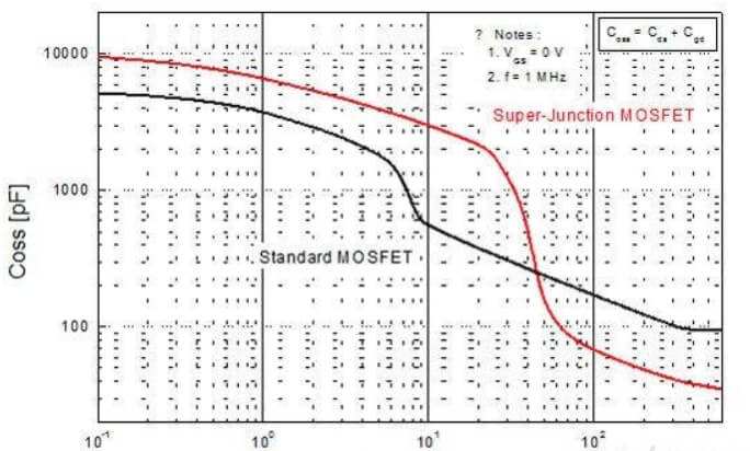
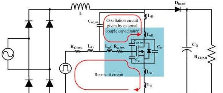
Because MOSFETs are unipolar devices, parasitic capacitance is the only limiting factor in switching transients. The charge balance principle reduces the on-resistance per specific area, and the chip size is smaller at the same RDS(ON) compared to standard MOSFET technology. Figure 1 shows the capacitance of a superjunction MOSFET and a standard planar MOSFET. The Coss of a standard MOSFET is a moderately linear variation, while the Coss curve of a superjunction MOSFET is highly nonlinear. The initial value of Coss for a superjunction MOSFET is higher because of the higher cell density, but in a superjunction MOSFET, Coss drops rapidly around a drain-source voltage of about 50V, as shown in Figure 2. When using superjunction MOSFETs for PFC or DC/DC converter applications, these nonlinear effects may cause voltage and current oscillations. Figure 3 shows a simplified PFC circuit diagram, including the internal parasitic components of the power MOSFET and the external oscillator circuit, which includes the external coupling capacitance Cgd_ext caused by the layout.
Comparison of output capacitance of planar MOSFET and superjunction MOSFET

Figure 2: Comparison of output capacitance of planar MOSFET and superjunction MOSFET
Generally speaking, there are multiple oscillator circuits that affect the switching characteristics of MOSFETs, including internal and external oscillator circuits. In the PFC circuit of Figure 3, L, Co and Dboost are the inductor, output capacitor and boost diode respectively. Cgs, Cgd_int and Cds are the parasitic capacitances of the power MOSFET. Ld1, Ls1 and Lg1 are the drain, source and gate bonding wires and pin inductances of the power MOSFET. Rg_int and Rg_ext are the internal gate resistance of the power MOSFET and the external gate drive resistance of the circuit. Cgd_ext is the parasitic gate-drain capacitance of the circuit. LD, LS and LG are the stray inductances of the drain, source and gate traces of the printed circuit board (PCB). When the MOSFET is turned on or off, the gate parasitic oscillation occurs in the resonant circuit through the gate-drain capacitance Cgd and the gate lead inductance Lg1.
Simplified diagram of PFC circuit including parasitic elements inside and outside the power MOSFET

Figure 3: Simplified diagram of PFC circuit including parasitic elements inside and outside the power MOSFET
Under resonant conditions (ωL=1/ωC), the oscillating voltage generated in the gate and source voltages is much larger than the driving voltage. The voltage oscillation caused by the change in resonance is proportional to the quality factor, Q (=ωL/R=1/ωCR). When the MOSFET is turned off, the network of drain parasitic inductance (LD+Ld1), gate-drain capacitance Cgd and gate lead inductance Lg1 causes the gate oscillation voltage. If the gate resistance (RG-ext.+Rg_int.) is very small, Q becomes large. In addition, the voltage drop across LS and the source stray inductance of Ls1 produce oscillations in the gate-source voltage, which can be expressed by expression (1). Parasitic oscillations may cause gate-source breakdown, undesirable EMI, large switching losses, gate control failure, and even MOSFET failure.

How to optimize PCB design to maximize the performance of superjunction MOSFETs
It is very important to optimize the circuit design to maximize the performance of superjunction MOSFETs without adverse effects.


