How to Make Flexible and Rigid-Flex PCB Assemblies?
Rigid boards are known for their joined-up look. While PCBs are in huge demand nowadays, flexible boards are the latest innovation in the industry. Flexible-rigid and flex-flex PCBs are the result.
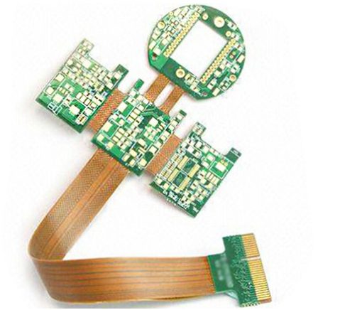
Rigid-flex PCB combine both rigid and flexible layers, while flex boards use only flexible materials. Flexible PCBs, on the other hand, allow for complete customization. Ultimately, the decision is up to you and your application needs.
Using flexible and rigid-flex PCBs offers the following advantages:
They can be used in a wide variety of situations.
The weight and size of the board can be reduced by using a high-density layout, where components are crammed into a small space.
The smaller and thinner boards you make will reduce the overall cost of your project, as they are cheaper than traditional PCBs.
The board already has a better security profile than standard PCBs.
How to Make Flexible PCBs?
In this section, we will take a look at the essentials of making flexible boards. Flexible circuits have specific properties of rigid printed circuit boards; however, the manufacturing process for each type of panel is quite different.
You must focus on the following:
Capabilities and procedures for handling thin materials
Preparation of specific pads
Production of polyimide cover films.
Material dimensional tolerances
Laser cutting of profiles
Electromagnetic smearing and etching
Capabilities and procedures for handling thin materials
Flexible PCB manufacturing is highly dependent on material management to provide high yields and reliable finished circuits. Handling is the cause of most scrap and reliability issues in the manufacturing process. Flexible materials are much thinner than rigid board materials and are not reinforced. Cover layers and flexible cores are typically 1.5-2 mils thick with copper thicknesses of 12 oz or 1 oz.
Flexible PCB Production Processing Materials
In order to transport flexible materials safely and without damage, a large portion of the process equipment must be customized for this purpose. In addition, employees must be taught how to properly handle themselves when performing manual labor. Any kinks or folds in the manufacturing panel can lead to scrapped components or reliability issues in the finished circuit.
Selective Pad Plating
An important production method is how and where copper is plated on the parts. Rigid-flex boards require the use of a pad plating technique that limits the amount of copper plating to the area inside the hole and a small circle around it.
No additional copper plating is applied to any traces. When designing at high density, it may be necessary to fully treat the circular area of the surface to obtain the best pad and trace imaging results.
Polyimide Cover Film Production
Solid polyimide sheets with adhesive backing are applied in the same way as solder mask and cover layers on rigid boards. However, because they are solid polyimide sheets, they must be manufactured using a separate manufacturing process.
All required apertures to expose SMT and PTH pads must be manufactured using laser cutting, drilling/planing, CNC knife cutting, punch and die sets, or a combination of these.
Material Dimensional Tolerances
Due to the need for flexibility, flexible materials are significantly thinner and do not require any additional support to maintain their shape (i.e. glass braid in rigid boards). This results in a material with much less dimensional stability, which must be accounted for in the tooling/registration systems used in production. Flexible materials can expand or contract when exposed to moisture, heat, and pressure.
To reduce the impact of material dimensional stability, smaller manufacturing panel sizes than rigid boards are often used,
Laser Cutting of Profiles
Polyimide materials can be easily cut by lasers. Therefore, very fine and complex profiles can be produced. At smaller manufacturing quantities, expensive hard punch and die tooling is not required, resulting in cost savings. Routing can be used, but the complexity of the profile will be limited and the edges of the components will be jagged. A sufficient amount of carbon residue will be left on the edges of the components after laser cutting, as required by IPC.
Electromagnetic Smearing and Etching
Desmear and etch-back processes are critical for reliable plated holes and inner layer interconnects in multi-layer flex systems.
Polyimide and flex adhesives used to hold the layers together have significantly different material properties than rigid boards. Standard chemistry-based etching techniques are too harsh for rigid boards. Ultimately, this leads to uneven results, reliability issues, and a limited and difficult to control process window. Plasma-based etching is the preferred method because it produces results with excellent quality and consistency.
Important Manufacturing Tips
Now we will see the important things involved in rigid-flex PCB manufacturing
Choosing the Right Materials
High-quality materials are essential if you want your printed circuit boards to perform at their best. Here are some of the materials needed to make flexible PCBs:
In terms of base material, polyimide is the best choice. It is more attractive with its combination of excellent characteristics and reasonable price.
The abbreviation of polyetheretherketone is PEEK. It is based on PEEK, but the content is not pure PEEK. We find this material used in complex applications due to its resistance to high temperatures and radiation.
Speaking of Teflon coated pans, polytetrafluoroethylene (PTFE) is the abbreviation of polytetrafluoroethylene. It can withstand extreme temperatures and dissipate heat with minimal loss. Other materials required to design the circuit board, such as cladding and conductive materials, should also be taken into consideration.
Conventional Equipment: How Do We Choose Rigid-Flex PCBs?
The performance and reliability of flexible PCBs will be significantly improved if assembled using high-tech machines. You can get the most outstanding design and materials. Unless you use current technology, your efforts will go to waste.
Only the best PCB companies employ skilled workers and the most advanced technology. Therefore, be sure to choose a company that is suitable for your product and manufactures the right type of circuit boards.
Importance of Stackup Management in Flex-Rigid PCBs
Stackup management is one of the most critical aspects of flexible PCB design. If you specify the stackup appropriately, the perfect assembly and performance of your board will be guaranteed. Put it this way, it sounds like a breeze. On the other hand, a precise stencil is not a simple task.
Stackup management relies heavily on expertise and understanding of the appropriate design software. You can only learn how to build a trustworthy PCB by experiencing and studying successful stackups yourself.
Printed circuit boards need to distinguish between two forms of flexibility:
Flexing in Motion
Since the product has standard flexibility, the board must be folded and bent every time it is used.
PCBs that can be mounted anywhere
As the name suggests, you only need flexibility and bendability during the entire installation process. Once the board is placed in the intended position, it is no longer possible to take advantage of its elastic properties.
If you compare the two panels, the design of the flexible mounting board is simpler, because only the mechanical stress of the ground plane needs to be considered when setting up the board.
The integrity of the signal and ground planes of the flexible PCB must be satisfactory under dynamic bending. Keeping in mind the integrity of the information while paying attention to the substrate material will be of great benefit.
Bend Management on Flex-Rigid PCBs
If you are using a flex layer on your board to carry ground planes and power, you should not only focus on trace routing. Those who choose designs that fold frequently also need to consider vias and surface mount pads.
Plated through holes are almost common when manufacturing flex PCBs. For pads, industry experts recommend using additional cover layers to secure them. This may enhance the durability and robustness of the board.
Vias and components should not be placed near the bend of a flex-rigid PCB. If the bend is repeatedly subjected to mechanical stress, the performance of adjacent vias and components may be affected. As a result, the reliability and durability of the board may be affected.
PCB Trace Management with Rigid-Flex PCBs
Finally, we will discuss how to layout your traces. Make sure to place them perpendicular to the curve. This is especially important in flex-rigid PCBs as it reduces trace stress. If your design is double-sided, consider offsetting your traces.
Stagger the traces on the bottom and top of the circuit. This way, you will be able to achieve greater uniformity and resilience to constant bending and mechanical stress. The strength and reliability of your board will be improved.
The impedance of the signal path should maintain a consistent value throughout the length of the trace. The goal is to find the right markings for the flex and rigid layers of your board.
The design of any type of PCB is where everything starts, as assembly may be more efficient there. You must take a close look at all the steps involved in manufacturing a flex-rigid or flexible PCB. Keep in mind that developing a rigid-flex PCB is more complex than a flexible PCB. Your PCB will perform better if you use the proper materials, control the stackup, etc.

