How to distinguish whether a PCB is single-layer or double-layer?
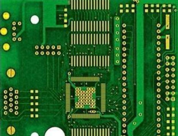
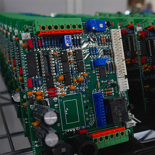
PCB physical object: A double-layer board has copper foil conductors on both sides.
Electronic version PCB: There are two colors of conductors (different colors of conductors represent different layers)

3 Double-layer PCB board design and wiring principles
The ground wire of the double-layer board is designed to be formed as a grid-shaped frame, that is, more parallel ground wires are laid on one side of the printed board, and the other side is the vertical ground wire of the copy board, and then they are connected with metalized vias at the intersection (the via resistance should be small).
In order to consider that a ground wire should be set near each IC chip, a ground wire is often laid every 1 to 115 cm. Such dense ground wires make the signal loop area smaller, which is conducive to reducing radiation. This ground grid design method should be before laying signal lines, otherwise it is difficult to implement.
Signal line wiring principles:
After the reasonable layout of the components of the double-layer board is determined, the ground grid copy board power line is designed first, and then the important lines-sensitive lines and high-frequency lines are laid, and then the general lines-low-frequency lines are laid. It is best for the key leads to have independent power supply, ground loop, and very short leads, so sometimes a ground line is laid next to the key line close to the signal line to form the smallest working loop.
The wiring principles of the top and bottom surfaces of the four-layer board are the same as the signal lines of the double-layer board. The key crystal, crystal oscillator circuit, clock circuit, CPU and other signal lines are laid first, and the principle of keeping the circulation area as small as possible must be followed.
When the PCB printed circuit IC circuit is working, the circulation area has been mentioned many times before. In fact, it comes from the concept of differential mode radiation. For example, the definition of differential mode radiation: the circuit working current flows in the signal loop, and this signal loop will generate electromagnetic radiation. Since this current is differential mode, the radiation generated by the signal loop is called differential mode radiation, and the calculation formula for its radiation field strength is:
E1=K1·f2·I·A/γ
Where: E1—the radiation field strength at the space γ of the differential mode copy board printed circuit board can be seen from the differential mode radiation formula. Its radiation field strength is proportional to the operating frequency f2, the circulation area A, and the operating current I. For example, when the operating frequency f is determined, the size of the circulation area is the key factor that can be directly controlled in our design. At the same time, the circulation working speed and current are not the larger the better as long as they meet the reliability. The narrower the signal jump edge and the lower jump edge, the larger and wider its harmonic component is, the higher the electromagnetic radiation is, and the larger the power is, the larger the current is (as mentioned above), which is what we do not expect.
The following are several reference values of the circulation area allowed by logic circuits that can meet the radiation Class B standard. It can be seen that the faster the circuit switching speed, the smaller the allowed area.
Key connections, if possible, can be surrounded by ground wires. After the PCB copy board is routed, all gaps can be covered with ground wires, but it must be noted that these covered ground wires must be short-circuited with the low-impedance joint of the large ground layer, so that good results can be achieved (Note: the gap requirements must meet the conditions, such as creepage distance, etc.).
4 Double-layer PCB board wiring skills
In the highly competitive market for battery-powered products, designers are always required to use double-layer circuit boards in their designs when considering target costs. Although multi-layer boards (four-layer, six-layer, and eight-layer) can do better in terms of size, noise, and performance, cost pressure forces engineers to use double-layer boards as much as possible. In this article, the concepts of current return paths with or without automatic routing, with or without ground planes, and the layout of parts on double-layer boards will be discussed.
It is attractive to use an automatic router to design printed circuit boards (PCBs). In most cases, automatic routing will not cause problems for purely digital circuits (especially low-frequency signals and low-density circuits). However, when trying to use the automatic routing tools provided by the routing software to route analog, mixed-signal or high-speed circuits, some problems may occur, and it may cause very serious circuit performance problems.
There are many things to consider about routing, but the more troublesome issue is the grounding method. If the ground path starts from the upper layer, the ground of each device is connected to the ground line through the pull line on that layer. For each device on the lower layer, the ground loop is formed by connecting the through hole on the right side of the circuit board to the upper layer. The immediate red flag that users will see when checking the routing method indicates that there are multiple ground loops. In addition, the ground loop on the lower layer is interrupted by a horizontal signal line. The only advantage of this ground structure is that the analog devices (MCP3202; 12-bit AD converter and MCP4125; 2.5V reference voltage) are concentrated on the right side of the circuit board. This arrangement ensures that the digital ground signal does not pass under these analog chips.
When using manual routing, follow the following design guidelines to ensure good results:
●Design the ground as a ground plane as a current return path.
●Separate the analog ground plane from the digital ground plane.
● If it is unavoidable to place the signal trace and the ground trace on the same layer, design the signal trace and the ground trace to be perpendicular to each other to reduce the interference of the signal trace on the ground current loop.
● Place the analog circuit next to the circuit board and the digital circuit system closest to the power supply. This can reduce the impact of digital switching δi/δt on the analog circuit.
However, it should be noted that both double-layer boards have a ground plane on the lower layer of the circuit board. This design allows engineers to quickly see the wiring when troubleshooting. This method often appears in the demonstration and evaluation boards of device manufacturers. However, a more typical practice is to lay a ground plane on the upper layer of the circuit board to reduce electromagnetic interference (EMI).
The existence of a current return path on the ground plane
The basic issues that should be considered when dealing with the current return path are:
(1) If only a wire is used as a ground line, make the wire as wide as possible; if only a wire is considered to be used as the ground line of the circuit board, the wire should be as wide as possible. The size of the thumb is a good standard, but it is also important to know that the minimum width of the ground wire refers to the effective copper foil width from the point to the end of the wire, where the “end” is defined as the point farthest from the power connection.
(2) Avoid forming a closed ground loop.
(3) If there is no ground plane, a star connection can be used.
If a ground plane cannot be designed, the current return path can be handled by a “star” wiring method.
In this way, the ground current of each device returns to the power supply end separately. Users will find that not all devices in Figure 5 have their own return path. U1 and U2 share the return path. The prerequisite for allowing this is to meet the following design points.
Do not pass digital circuits through analog devices.
During switching, digital circuits will form a relatively large current in the ground loop, but the time is very short. This phenomenon is caused by the equivalent inductance and resistance of the ground loop. The inductance of the ground plane or ground wire will produce a voltage drop of V = Lδi/δt, where L is the equivalent inductance of the ground plane or ground wire, δi is the change in current from the digital device and δt is the time of current change. The voltage change caused by the equivalent resistance of the ground plane or ground wire is V = RI, R is the equivalent resistance of the ground plane or ground wire, and I is the current change of the digital device. This voltage change of the ground plane or ground wire will affect the normal signal between the input terminal of the analog device and the ground.
Don’t let high-speed current pass through low-speed devices
The change of the ground return signal of the high-speed circuit on the ground plane has a similar effect as described above. The formula that determines this interference effect is: V = Lδi/δt for the equivalent inductance of the ground plane or ground wire, and V = RI for the equivalent resistance of the ground plane or ground wire. When the ground plane or ground wire of the digital circuit or high-speed circuit passes through the pull line of the analog device, it will cause a change in the signal between the input terminal of the analog device and the ground. Regardless of the technology used, the equivalent resistance and inductance of the ground return path must be designed to be minimized. If a ground plane is used, cutting the ground plane may improve or degrade the performance of the circuit, so use it with caution.
Sometimes a continuous ground plane is less effective than an isolated ground plane. The ground routing method shown in (a) is less effective than that shown in (b).
The precise analog is closer to the connector, but it is isolated from the digital circuits and the switching currents from the power supply circuit. This is an effective way to separate the ground return path.
Conclusion
When discussing wiring-related technologies, two issues will be discussed: What if management cannot use a double-layer board or a ground plane, but still needs to reduce the noise in the circuit? And how to design the circuit to meet the ground plane requirements? Generally speaking, the solution is to tell management that a ground plane is necessary if reliable circuit performance is to be achieved. The main reason for using a ground plane is that the ground impedance is low and it can reduce EMI to a certain extent. But if cost constraints prevent users from achieving what they need, some suggestions provided in this article, such as star networks and correct current return paths, can also slightly reduce circuit noise.
KKPCB provides global customers with one-stop services from PCB layout, prototype PCB proofing, PCB manufacturing, PCBA processing (including SMT and DIP), PCBA testing, PCBA product assembly and outbound packaging. You could provide a Gerber file or BOM list to us, we will offer the finished PCB products or PCB assembly which are satisfied with you.


